Electromagnetic induction type liquid crystal panel as well as manufacture method thereof and liquid crystal display (LCD)
A liquid crystal panel and electromagnetic induction technology, which is applied in the field of liquid crystal display and electromagnetic induction liquid crystal panel, can solve the problems of reduced input accuracy, decreased input accuracy, and infirmity, so as to improve accuracy and reliability, reduce assembly cost, and meet light and thin requirements. effect
- Summary
- Abstract
- Description
- Claims
- Application Information
AI Technical Summary
Problems solved by technology
Method used
Image
Examples
no. 1 example
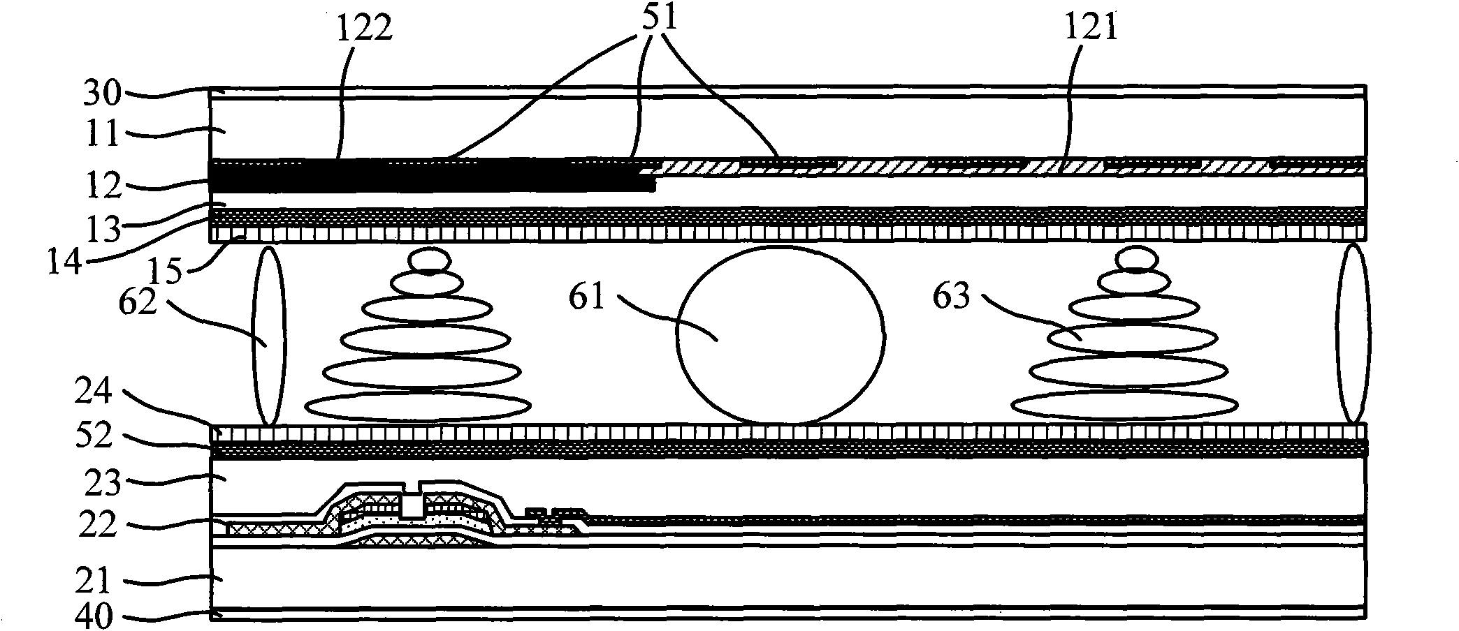
[0033] figure 1 It is a partial side view structural diagram of the electromagnetic induction type liquid crystal panel provided by the first embodiment of the present invention. The plane of the liquid crystal panel is usually divided into a plurality of pixel units. This embodiment takes a typical thin film transistor liquid crystal display as an example for description, such as figure 1 Shown is the structure of a pixel unit in a liquid crystal panel.
[0034] A typical multi-layer structure on a color filter substrate starts from the side adjacent to the first base substrate 11, and at least sequentially includes a color resin and black matrix layer 12, a first protective layer 13, a common electrode layer 14 and a first orientation 膜层15。 Film layer 15. The color resin and black matrix layer 12 includes a color film resin 121 and a black matrix 122, and the black matrix 122 is arranged between the color film resin 121 at intervals. The first protective layer 13 is generally m...
no. 2 example
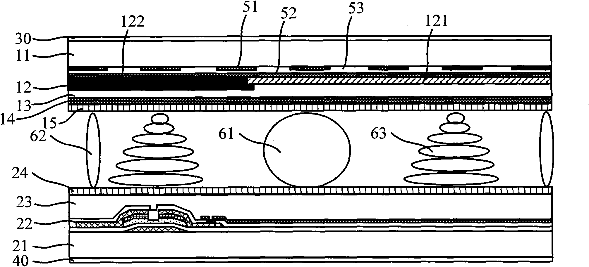
[0047] In the second embodiment of the present invention, the structure of the liquid crystal panel is basically the same as that of the first embodiment. The antenna array includes first-direction wires and second-direction wires that are perpendicular to each other. The difference is: the first-direction wires and the second-direction wires are covered There is an insulating transparent film layer, that is, when the first direction wire and the second direction wire are formed into the liquid crystal panel, an insulating transparent film layer can be provided on both sides of the first direction wire and the second direction wire to ensure the first direction wire And the second direction wire is insulated from the liquid crystal panel.
[0048] In this embodiment, the first-direction wire 51 and the second-direction wire 52 may be formed with an inner space insulating layer 53, and the first-direction wire 51 and the second-direction wire 52 are insulated first.
[0049] The ant...
no. 3 example
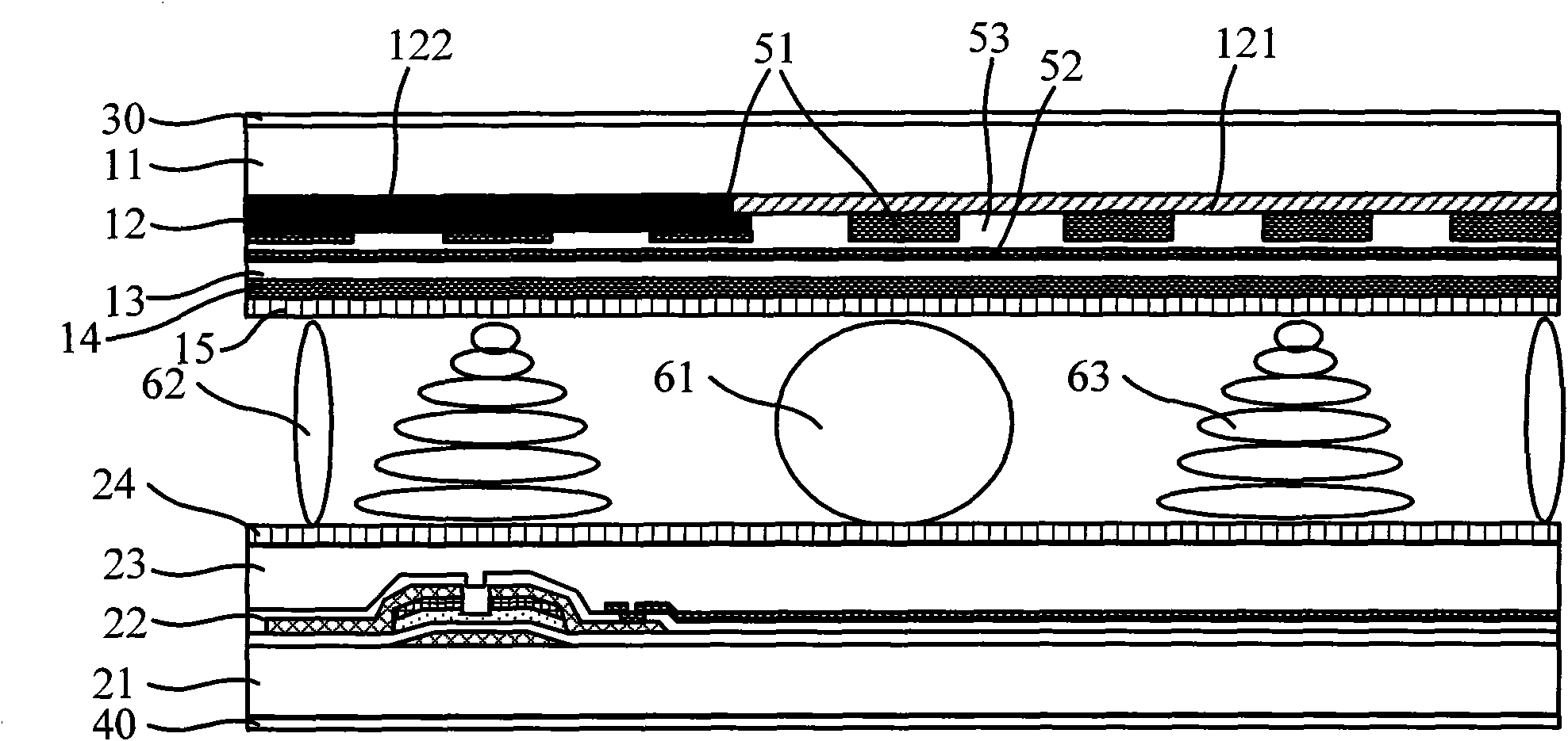
[0054] In the third embodiment of the present invention, the structure of the liquid crystal panel is basically the same as that of the first embodiment. The antenna array includes first-direction wires and second-direction wires that are perpendicular to each other. The difference is: first-direction wires and / or second-direction wires The upper is covered with an outer space insulating layer, so as to ensure the insulation between the first direction wire and the second direction wire and the conductive material in the liquid crystal panel.
[0055] By adopting the above technical solution, the first-direction wires and the second-direction wires can be arranged at any position in the two base substrates of the liquid crystal panel, and can be arranged together so that the insulating layer is kept insulated within the space, or they can be arranged separately. Still taking the typical color filter substrates and array substrates described in the above embodiments as examples for...
PUM
 Abstract
Description
Claims
Application Information


