

Mounting substrate, and method for manufacturing thin light-emitting device using same
A technology for mounting a substrate and a manufacturing method, which is applied in the directions of electrical components, electric solid-state devices, circuits, etc., can solve problems such as hindering stability, impairing appearance, and short-circuiting, and achieves the effect of easy handling
- Summary
- Abstract
- Description
- Claims
- Application Information
AI Technical Summary
Problems solved by technology
Method used
Image

Examples
Embodiment Construction
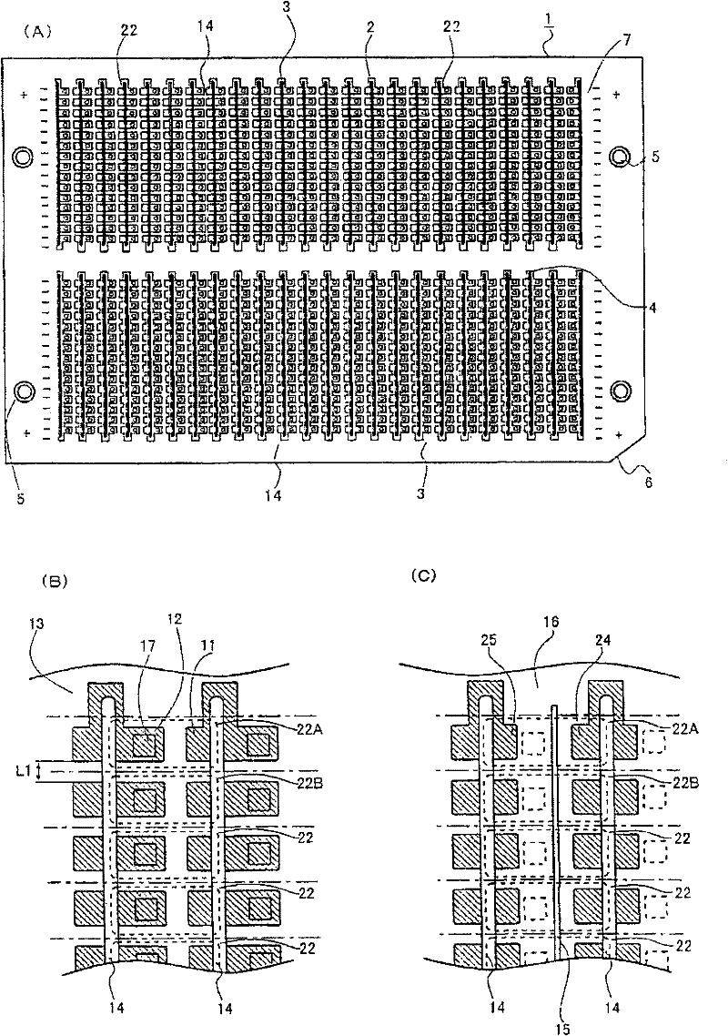
[0040] Below, refer to Figure 1 to Figure 6 Embodiments of the present invention will be described.
[0041] first, figure 1 Shows the mounting substrate of the present invention. figure 1 (A) is a plan view, figure 1 (B) is an enlarged view of the surface, figure 1 (C) is an enlarged view of the back side.
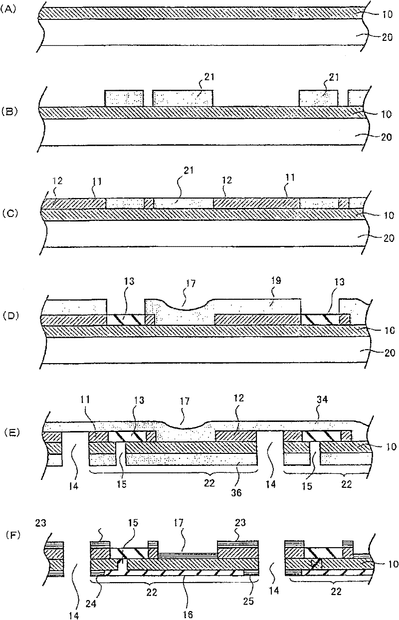
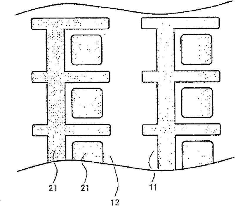
[0042] The mounting substrate 1 of this embodiment is composed of a conductive foil 10 , a first electrode portion 11 , a second electrode portion 12 , a liquid resin 13 , a separation slit 14 , an insulation slit 15 , and a solder resist layer 16 .
[0043] As the conductive foil 10 , a metal that can be etched and electrolytically plated is selected. In this embodiment, metal foil made of copper is used. Copper foils with extremely thin thicknesses such as 9 μm, 12 μm, 18 μm, and 35 μm are selected. This is because copper foils constitute the mounting substrate of thin light-emitting devices, so it is better to choose copper foils as thin as possible. If the...
PUM
 Abstract
Description
Claims
Application Information