Electronic component transporting device

A technology of electronic components and transmission devices, applied in the direction of electrical components, electrical components, circuits, etc.

Active Publication Date: 2011-01-12
MURATA MFG CO LTD
View PDF9 Cites 21 Cited by
  • Summary
  • Abstract
  • Description
  • Claims
  • Application Information

AI Technical Summary

Problems solved by technology

That is, even if the diameter of the above-mentioned cylindrical member 1002 is within a predetermined range, the electronic components 1003 arranged in a predetermined direction may deviate from the predetermined direction again due to vibration.

Method used


Image

  • Electronic component transporting device
  • Electronic component transporting device
  • Electronic component transporting device

Examples


no. 1 approach

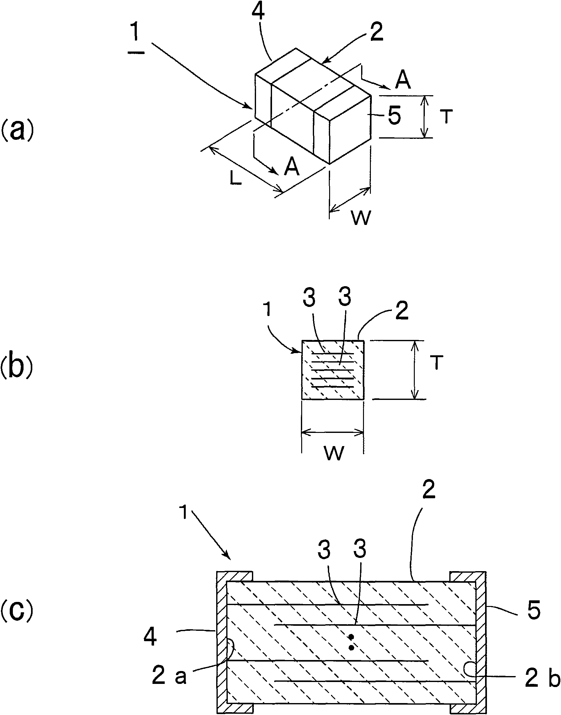
[0057] image 3 (a) is a perspective view of the electronic component conveyed in 1st Embodiment of this invention. The electronic component 1 is a multilayer ceramic capacitor and has a rectangular parallelepiped shape. That is, electronic component 1 has rectangular parallelepiped ceramic sintered body 2 . Such as image 3 As shown in (b) and (c), in the ceramic sintered body 2, a plurality of internal electrodes 3 are laminated via a ceramic layer. In the present embodiment, the internal electrode 3 is mainly composed of nickel and has strong magnetism. The internal electrodes of the electronic component which is the object of the present invention can be made of suitable materials as long as they have strong magnetism.

[0058] The first and second external electrodes are formed so as to cover the first and second end faces 2 a and 2 b of the ceramic sintered body 2 facing each other. The direction connecting the first end face and the second end face 2a, 2b of the el...

no. 2 approach

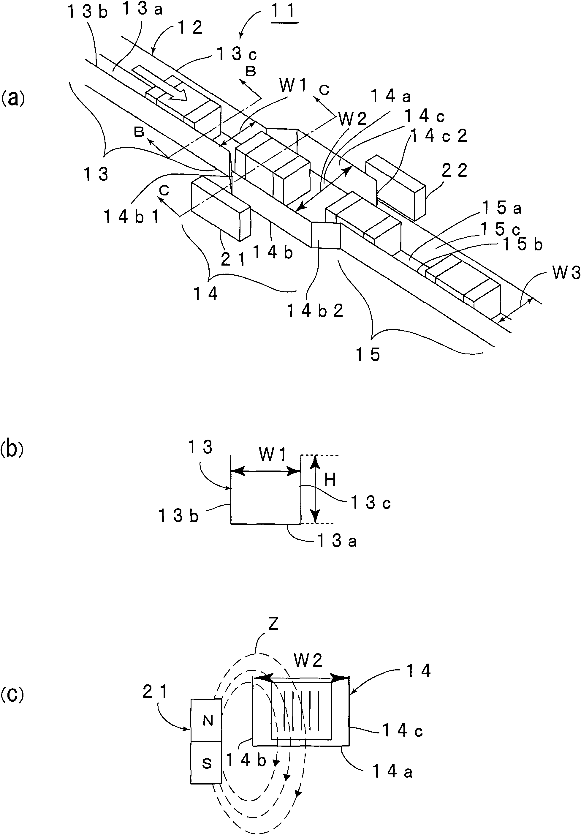
[0108] In the first embodiment, the first magnet 21 is located outside the guide wall 14b, with the N pole on the upper side and the S pole on the lower side.

[0109] Unlike this, as Figure 5 As shown, in the second embodiment, the first magnet 21A is arranged below the rotation path 14, more specifically, below the second transfer table 14a. The upper surface of the first magnet 21A is an N pole, and the lower surface is an S pole. Therefore, yielding Figure 6 The magnetic lines of force Z shown. Since the magnetic field lines Z extending substantially in the vertical direction are generated on both the guide wall 14b side and the guide wall 14c side, as in the case of the first embodiment, the orientation of the electronic component 1 is aligned so that the surface direction of the internal electrodes 3 is vertically vertical. direction extension.

[0110] Since the first magnet 21A is located below the central position in the width direction of the second transfer ta...

no. 3 approach

[0112] Such as Figure 7 As shown, in the electronic component transfer device of the third embodiment, in addition to the first magnet 21A, another first magnet 21B is provided. That is, in the second embodiment, the first magnet 21A is provided below the second transfer table 14a, and in the third embodiment, the first magnet 21B is provided above it. In this way, the rotation path 14 is pinched by the upper and lower first magnets 21A, 21B.

[0113] Such as Figure 8 As shown, the upper side of the first magnet 21B is the N pole, and the lower side is the S pole.

[0114] In this way, if Figure 8 As shown, the first magnet 21B is arranged above the rotation path 14, and the magnetic lines of force Z from the first magnet 21B also act, so the electronic component 1 can be rotated more reliably and its orientation is consistent.

[0115] By adjusting the position of the first magnet 21B with respect to the position of the first magnet 21A, the arrangement of the lines of...


PUM


Abstract

The invention provides an electronic component transporting device, which can guide a plurality of electronic elements towards one direction, keep the position of the inner electrodes as the same and transport in order. The electronic component transporting device is a transporting device for transporting a rectangular electronic element (1) having ferromagnetic inner electrodes. The device is provided with a first transporting path (13), a rotating path (14) and a second transporting path (15), wherein each path is provided with first, second and third transporting platforms. A first magnet (21) is arranged in the rotating path (14) for exerting magnetic force lines on the electronic element (1) so as to guide the inner electrodes of the electronic element to face towards the specified direction.

Description

technical field [0001] The present invention relates to an electronic component conveying device for arranging and conveying electronic components in a predetermined direction, in particular to an electronic component conveying device for conveying and arranging electronic components whose internal electrodes are ferromagnetic. Background technique [0002] It turns out that when manufacturing electronic components such as ceramic electronic components, it is required to arrange the electronic components in a specified direction. For example, when marking the outer surface of electronic components or performing visual inspection or characteristic inspection, the electronic components must be aligned in a prescribed direction. [0003] In addition, when the final electronic components are mounted on the printed circuit board, the electronic components must also be arranged neatly. For example, a multilayer ceramic capacitor is formed by arranging a plurality of internal elec...

Claims


Application Information

Patent Timeline
Patent Type & Authority Applications(China)
IPC IPC(8): B65G47/24H01G13/00H01G4/30
CPCH01L21/68H05K13/0015
Inventor 三井肇松本浩高桥晴夫池田正仁青野隆之
Owner MURATA MFG CO LTD
Why Eureka
Try Eureka