Semiconductor packaging structure and semiconductor packaging process

A packaging process and packaging structure technology, applied in the direction of semiconductor devices, semiconductor/solid-state device manufacturing, semiconductor/solid-state device components, etc., can solve the problems of space occupation and cannot be effectively used, and achieve the effect of improving contact density

Active Publication Date: 2011-01-12
ADVANCED SEMICON ENG INC
View PDF5 Cites 6 Cited by
  • Summary
  • Abstract
  • Description
  • Claims
  • Application Information

AI Technical Summary

Problems solved by technology

[0005] Although the pins 124 are arranged in an area array on the periphery of the chip 110, the space under the chip 110 is still occupied by the chip pad 122 and cannot be effectively utilized.

Method used


Image

  • Semiconductor packaging structure and semiconductor packaging process
  • Semiconductor packaging structure and semiconductor packaging process
  • Semiconductor packaging structure and semiconductor packaging process

Examples


Embodiment Construction

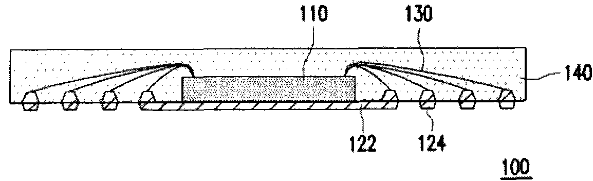
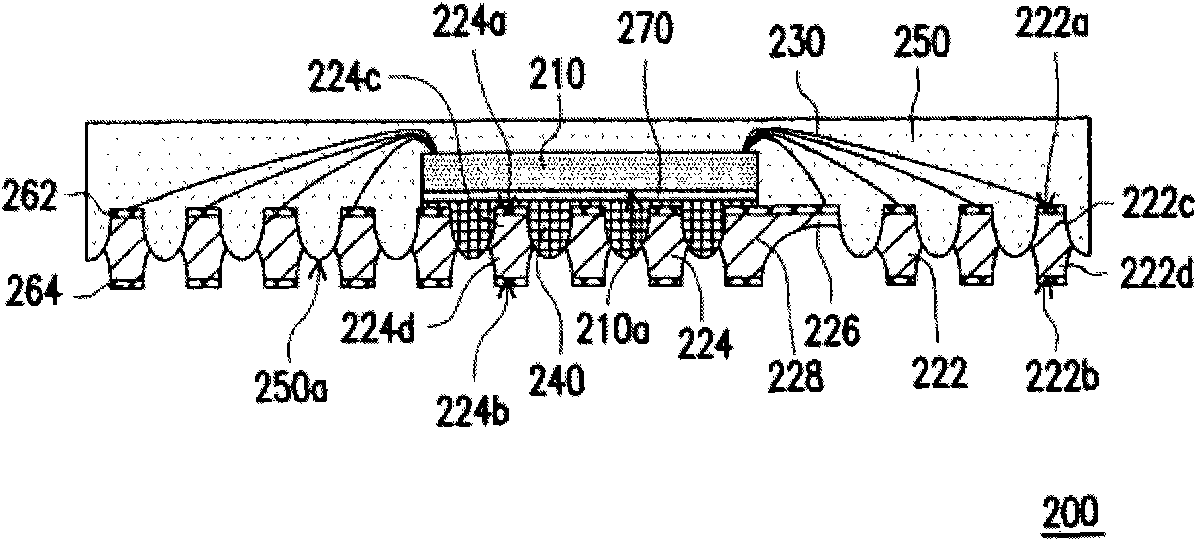
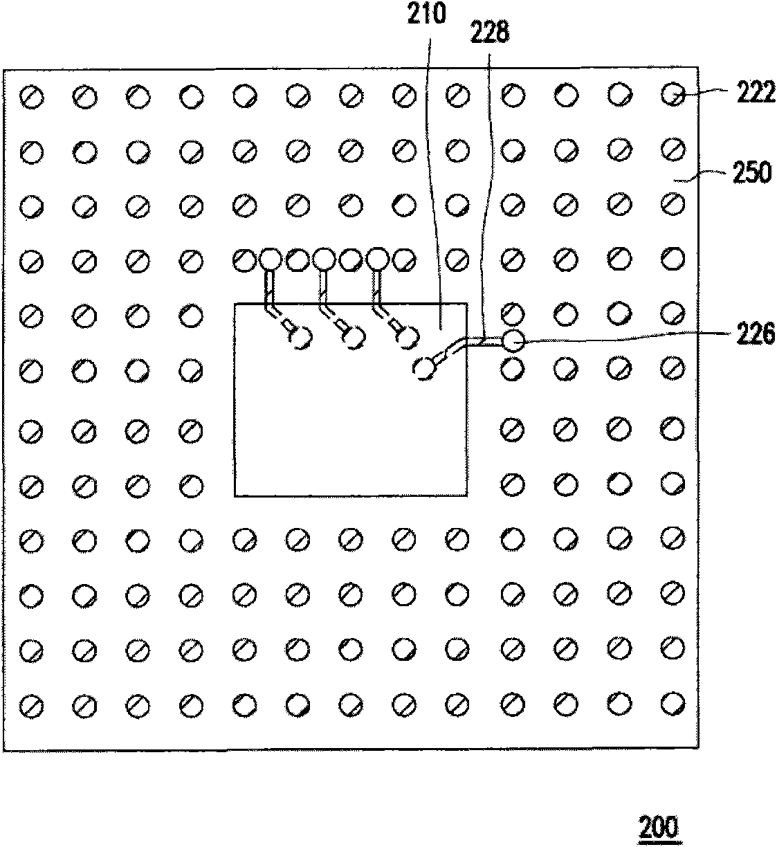
[0075] Reference will now be made in detail to some embodiments of the invention, examples of which are illustrated in the accompanying drawings. Wherever possible, the same reference numbers will be used throughout the drawings and this specification to refer to the same or like parts.

[0076] definition

[0077] Some or all of the following definitions apply to the embodiments described below.

[0078] As noted hereinafter, the singular forms "a", "an" and "the" include plural referents unless the context clearly dictates otherwise. For example, "a depression" may actually include multiple depressions.

[0079] As described hereinafter, the term "adjacent" means close to or adjacent to. Adjacent components may be spaced apart from each other or may be in actual or direct contact with each other. In some cases, adjacent components may be connected to each other or may be integrally formed with each other.

[0080] As described below, terms such as "inside", "top", "bott...


PUM


Abstract

The invention relates to a semiconductor packaging structure and a semiconductor packaging process. The semiconductor packaging structure has a full-array design, a first pin is arranged on the periphery of a chip and a second pin used as a contact is further arranged below the chip so that the space below the chip can be effectively utilized to improve the density of the contact of the semiconductor packaging structure. The invention also relates to a process of the semiconductor packaging structure.

Description

technical field [0001] The invention relates to an electronic device package. More specifically, the present invention relates to an advanced quad flat no-lead (aQFN) package structure and a manufacturing method thereof. Background technique [0002] In the market of radio frequency (radio frequency, RF), wireless, portable applications and personal computer (PC) peripherals, it is generally necessary to improve the performance of smaller packages and increase input or output (input / output, I / O ) is in high demand. For example, quad flat no-lead (QFN) packages have been widely accepted and are generally suitable for chip packaging involving high frequency transmission, such as via RF bandwidth. [0003] For the QFN package structure, the die pad and the surrounding leads are usually made of a wire bonding frame. The QFN package structure is usually soldered to a printed circuit board (PCB) through surface mounting technology (SMT). Therefore, the chip pads and leads of t...

Claims


Application Information

Patent Timeline
Patent Type & Authority Applications(China)
IPC IPC(8): H01L23/488H01L21/50
CPCH01L24/32H01L2224/48091H01L2224/48247H01L2224/73265H01L2224/83192H01L2224/83385H01L2924/181H01L2224/32245H01L2924/00014H01L2924/00012H01L2924/00
Inventor 廖国成
Owner ADVANCED SEMICON ENG INC
Why Eureka
Try Eureka