Battery silicon wafer detection system

A detection system and battery silicon wafer technology, applied in the field of detection systems, can solve the problems of increased probability, detection time, cost, inability to detect, and sort, etc., and achieve the effect of easy operation

Active Publication Date: 2012-09-05
武汉中导光电设备有限公司
View PDF0 Cites 0 Cited by
  • Summary
  • Abstract
  • Description
  • Claims
  • Application Information

AI Technical Summary

Problems solved by technology

However, the existing solar cell silicon wafer inspection system cannot complete the inspection and sorting on one conveying device, which increases the probability of defects, inspection time and cost

Method used


Image

  • Battery silicon wafer detection system
  • Battery silicon wafer detection system
  • Battery silicon wafer detection system

Examples


Embodiment Construction

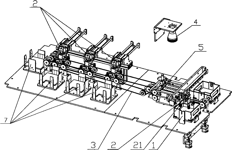
[0028] figure 1 It is a three-dimensional structural schematic diagram of the battery silicon wafer inspection system according to the present invention. From right to left in the figure, along the silicon wafer conveyor belt, there are feeding area, exposure area, inspection waiting area, and sorting area. The feeding area includes the feeding area Box 1 and manipulator 2, the front panel 11 of the two loading boxes 1 can be opened around the shaft at the bottom of the loading box 1, and the silicon wafer can be placed in the loading box 1 by hand, and the manipulator 2 picks up the silicon wafer through the suction cup 21 and Put it on the conveyor belt 3, and the silicon wafer is known by the electric control and UI after being placed on the conveyor belt 3, and the silicon wafer is transported to the exposure area by the conveyor belt 3.

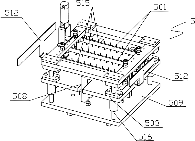
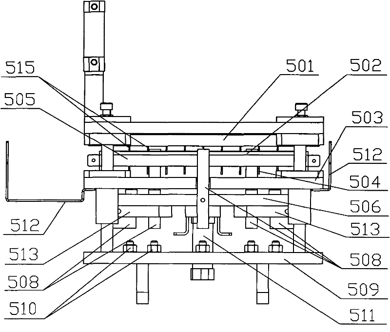
[0029] An imaging system is provided on the exposure area, and the imaging system is an imaging lens 4, and an electroluminescence limi...


PUM


Abstract

The invention relates to a detection system, in particular to a battery silicon wafer detection system, which comprises a silicon wafer conveying device, a feeding region, an exposing region and a sorting region, wherein the feeding region, the exposing region and the sorting region are sequentially arranged along the silicon wafer conveying device, the feeding region is used for placing silicon wafers on the silicon wafer conveying device; the exposing region is provided with a detection imaging system arranged above the silicon wafers and a limit mechanism used for limiting the silicon wafer; and the sorting region is used for placing silicon wafers with different masses in corresponding collecting boxes. Only by placing the silicon wafers into a feeding box of the feeding region, the invention can realize the sorting of the silicon wafers, which is simple and practical. A battery silicon wafer limiting mechanism is designed aiming at the electro-fluorescence principle, thus the silicon wafers are accurately fixed.

Description

[0001] This patent application is a divisional application. The filing date of the original application is: June 12, 2009, the application number is: 200910149174.3, and the name of the invention is: solar cell silicon wafer detection system. technical field [0002] The invention relates to a detection system, in particular to a battery silicon wafer detection system. Background technique [0003] The main components of solar panels are solar silicon wafers. The photoelectric conversion efficiency of solar silicon wafers has been continuously improved. It has extremely important applications in civil, national defense, aviation, aerospace and other aspects, and has become an indispensable member of clean energy. One, the industry has a strong demand for solar silicon wafers. Due to the thinness of solar silicon wafers, in the automatic manufacturing and testing process, if there is a slight carelessness, it may cause damage, missing corners or even tiny cracks that cannot b...

Claims


Application Information

Patent Timeline
Patent Type & Authority Patents(China)
IPC IPC(8): G01N21/64G01N21/88B07C5/342
Inventor 裴世铀李波杨铁成樊思民陈利平
Owner 武汉中导光电设备有限公司
Why Eureka
Try Eureka