

Semiconductor device, basic cell and semiconductor integrated circuit device
A basic unit and integrated circuit technology, applied in the direction of semiconductor devices, semiconductor/solid-state device manufacturing, semiconductor/solid-state device components, etc., can solve the problem of metal filling rate decline, so as to suppress the decline of manufacturing yield and suppress the through-hole metal The effect of the drop in fill rate
- Summary
- Abstract
- Description
- Claims
- Application Information
AI Technical Summary
Problems solved by technology
Method used
Image

Examples
no. 1 Embodiment approach
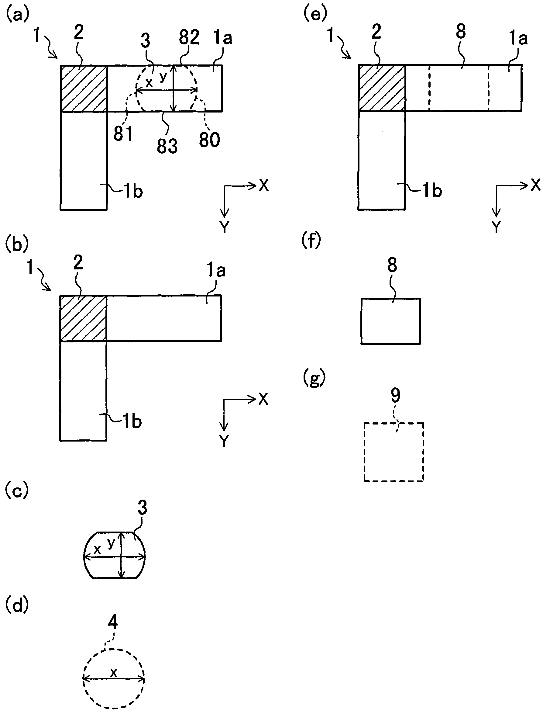
[0088] figure 1 It is a configuration diagram showing wiring and vias under wiring according to the first embodiment. In this figure, (a) is a plan view showing the arrangement position and shape of the wiring 1 and the via hole 3 below it, (b) is a plan view showing the shape of the wiring 1 alone, and (c) is a plan view showing the through hole 3 alone. (d) is a via pattern 4 used to mask the via hole 3 in the manufacture of a semiconductor device, (e) is a plan view showing the arrangement position and shape of the wiring 1 and the via hole 8 below it. , (f) is a plan view showing the shape of the via hole 8 alone, and (g) is a via hole pattern 9 used for mask formation of the via hole 8 at the time of semiconductor device manufacture.
[0089] In the wiring of a semiconductor device, there are generally a plurality of curved regions, that is, bent portions 2 , on the wiring path. For example figure 1 As shown in (b), the L-shaped wiring 1 as the first wiring has a ben...
no. 2 Embodiment approach
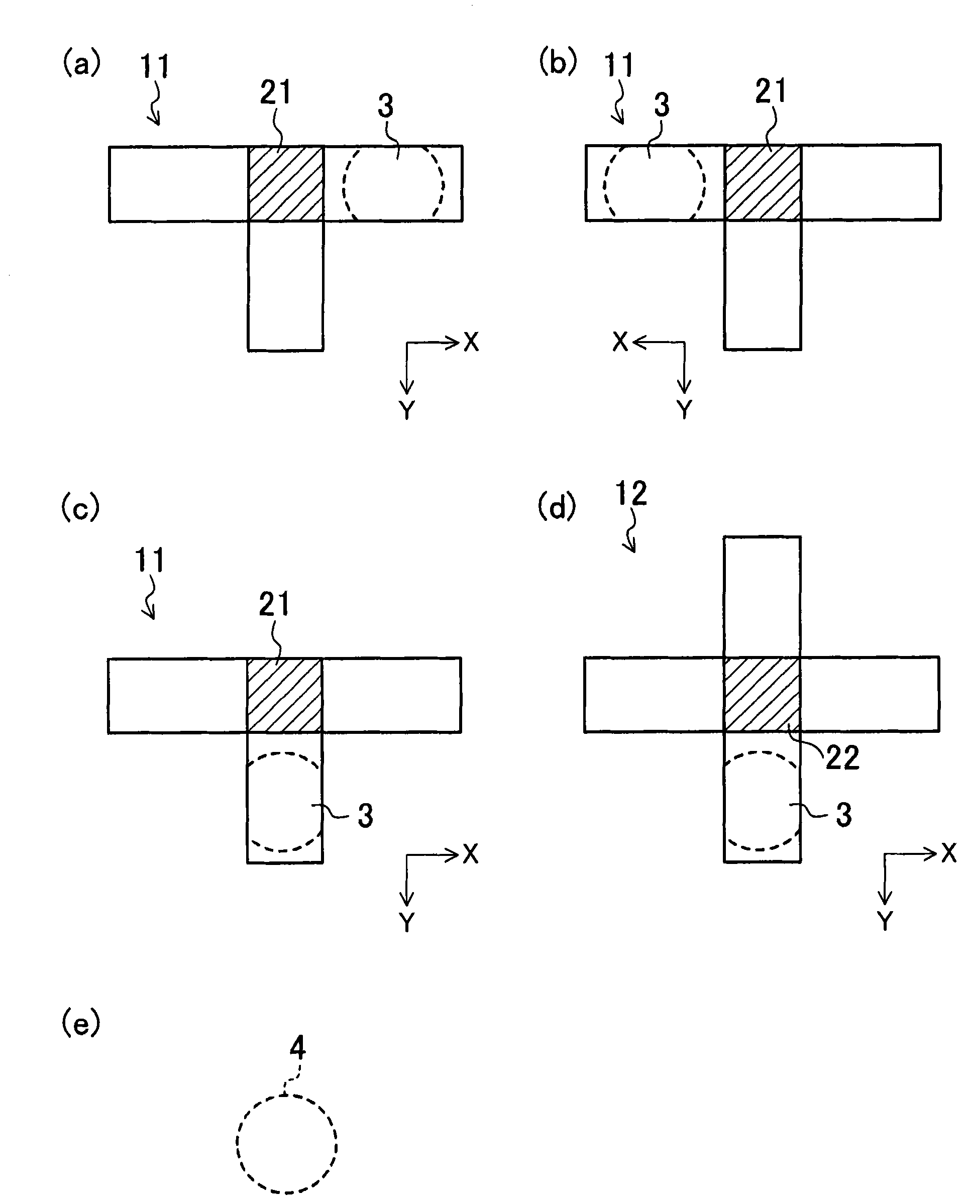
[0099] image 3 It is a configuration diagram showing wiring and vias under wiring according to the second embodiment. In this figure, (a) is a plan view showing the arrangement position and shape of the wiring 1 and the via holes 3 and 31 therebelow, (b) is a plan view showing the shape of the wiring 1 alone, and (c) is showing the through hole. 3, 31 is a plan view of the shape of a single body, (d) is a via hole pattern used for mask formation of the via holes 3, 31 in the manufacture of a semiconductor device. image 3 structure with figure 1 roughly the same as figure 1 The same structural elements are attached to the figure 1 same symbol.
[0100] exist image 3 In the structure of , between the wiring 1 and the second wiring (not shown) arranged under the wiring 1, a via 31 as a second via is formed in addition to the via 3 so that the via 31 includes a bend. Section 2 area. The through hole 31 has the notch part 5 similarly to the conventional through hole. ...
no. 3 Embodiment approach
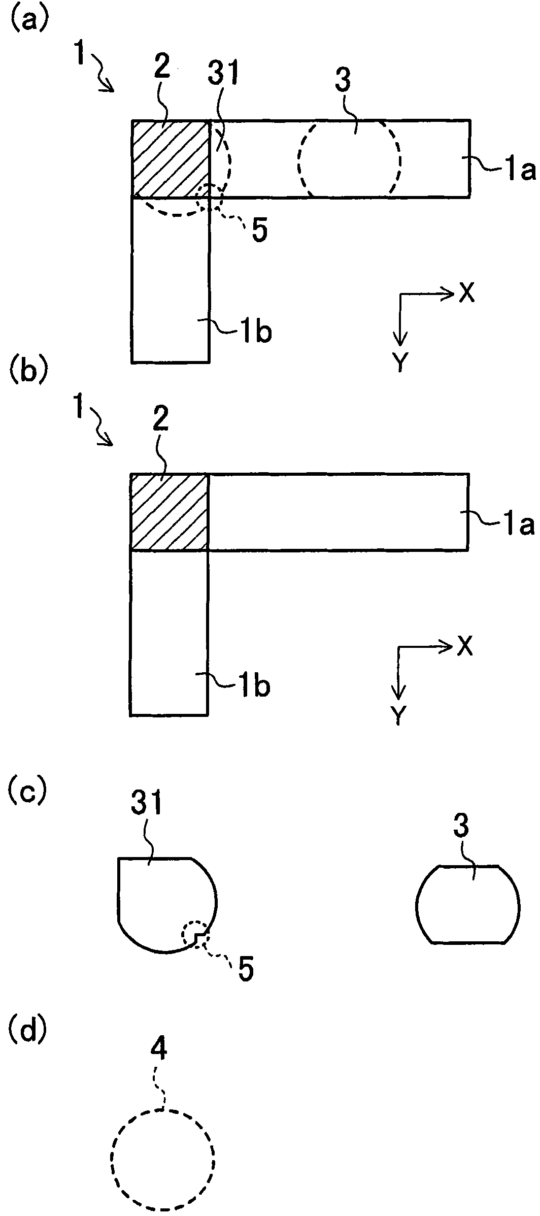
[0104] Figure 5 It is a configuration diagram showing the wiring and the via hole under the wiring according to the third embodiment. In this figure, (a) is a plan view showing the arrangement position and shape of the wiring 13 and the through hole 41 below it, (b) is a plan view showing the shape of the wiring 13 alone, and (c) is a plan view showing the shape of the through hole 41 alone. In the plan view of the body shape, (d) is a via pattern 4 used for masking the via hole 41 during semiconductor device manufacture, and (e) to (g) are plan views showing examples of other wiring shapes.
[0105] exist Figure 5 In the structure of , between the wiring 13 as the first wiring and the second wiring (not shown) arranged in the lower layer of the wiring 13, using Figure 5 The circular through hole pattern 4 shown in (d) is larger than the bent portion 2 to form a through hole 41 as a first through hole.
[0106] Such as Figure 5 As shown in (b), the wiring 13 has a bent...
PUM
 Abstract
Description
Claims
Application Information