Processing apparatus and method of manufacturing electron emission element and organic el display

A technology for processing devices and processing objects, which is applied to electrical components, lighting devices, electric solid devices, etc., can solve problems such as cost increase, degree of freedom limitation, device design freedom degree, expansion limitation, etc., to avoid scars, easy Coping effect

Inactive Publication Date: 2011-02-09
CANON ANELVA CORP
View PDF6 Cites 11 Cited by
  • Summary
  • Abstract
  • Description
  • Claims
  • Application Information

AI Technical Summary

Problems solved by technology

[0039] In this way, when glass is used as the object of film formation, additional countermeasures are required, and as a result, new problems such as increased production tact of the device and increased cost arise.
[0040] In addition, since the step of improving the adhesion between the mask and the object to be processed disclosed in Patent Document 6 is fixed sequentially from one end all the time, the degree of freedom when the size of the object to be processed is changed is limited. limit such problems
[0041] In particular, when coping with the increase in width of the substrate to be processed, there is a problem that the design freedom and expandability of the device are limited.

Method used


Image

  • Processing apparatus and method of manufacturing electron emission element and organic el display
  • Processing apparatus and method of manufacturing electron emission element and organic el display
  • Processing apparatus and method of manufacturing electron emission element and organic el display

Examples


Embodiment Construction

[0057] Embodiments of the present invention will be described below with reference to the drawings. Here, vapor deposition treatment is taken as an example of treatment, but the treatment of the present invention is not limited thereto.

[0058] This application relates to an invention related to a processing device for applying tension to a film-like plane of the mask in which a mask used is formed of a thin-film magnetic material.

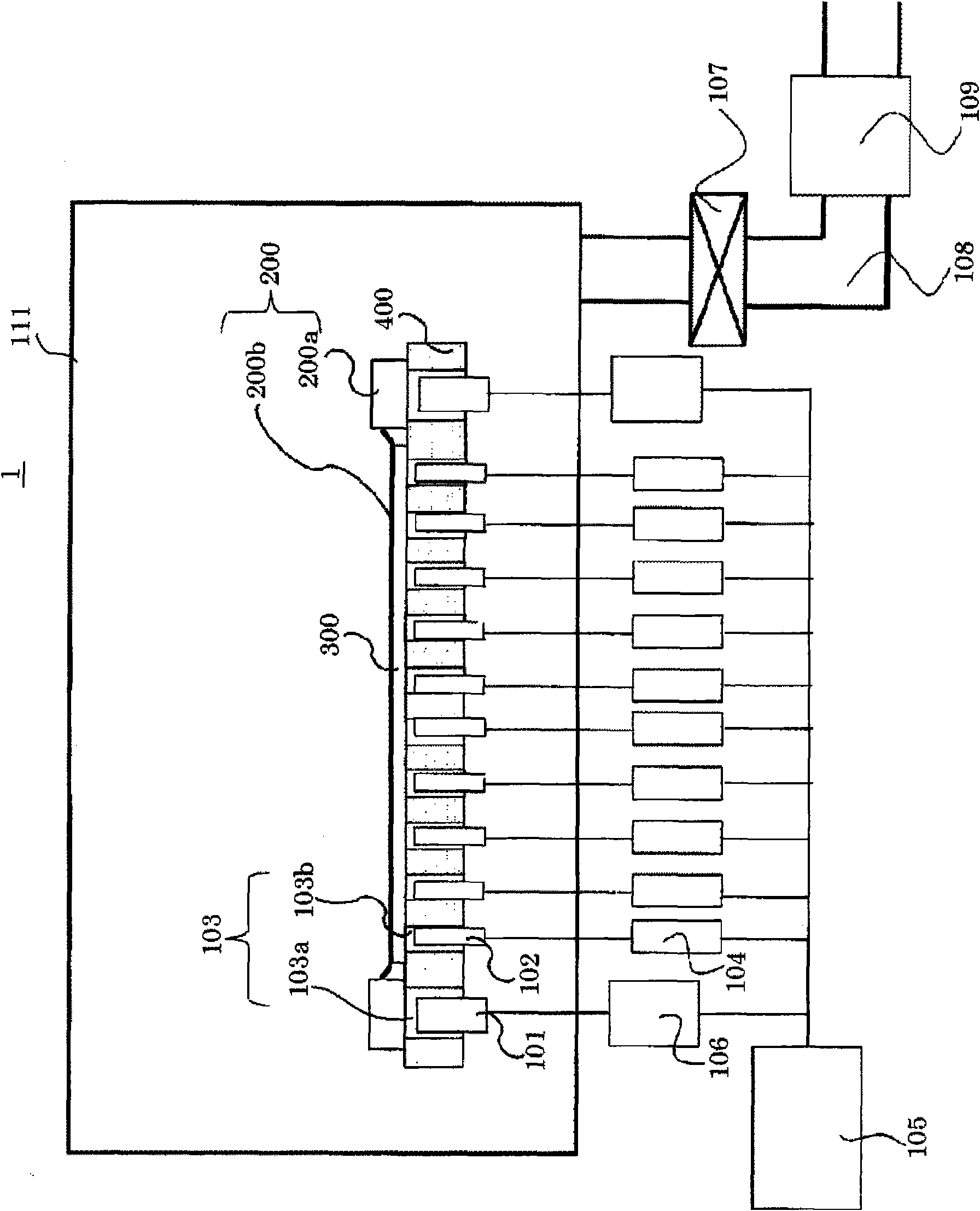
[0059] figure 1 It is a schematic diagram of the processing apparatus of this invention.

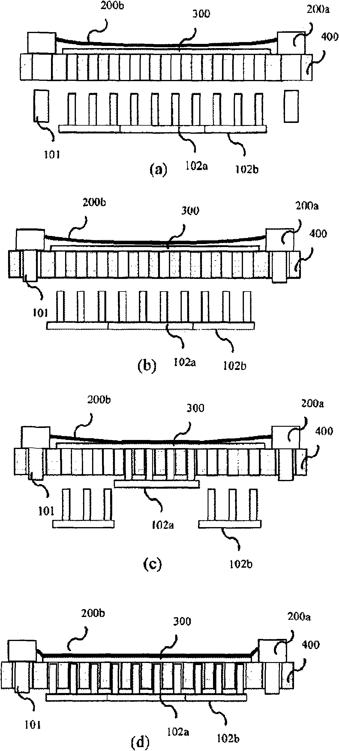
[0060] This figure shows the state after the mask fixing operation described later. During vapor deposition, the mask fixing device is turned upside down, and vapor deposition is performed with the processing surface of the mask and the substrate facing downward.

[0061] Reference numeral 1 in the figure is a processing device, reference numeral 101 is a fixing member (second fixing member) of the mask frame 200a, and reference numeral 102 is a mask mem...


PUM

PropertyMeasurementUnit
thicknessaaaaaaaaaa

Abstract

Highly accurate batch pattern film formation is made possible even when using a mask, which has a possibility of deteriorating pattern alignment accuracy due to heavy weight as a result of meeting the requirement of size increase of a subject to be processed. Specifically, a processing apparatus (1), which performs processing by fixing a subject (300) to be processed and a mask (200), is provided with a base (400) for placing the subject (300) and the mask (200). Furthermore, the processing apparatus is provided with a second fixing means (101), which includes a permanent magnet for fixing a mask frame (200a) of the mask (200) on the base (400). The processing apparatus is also provided with a first fixing means (102), which includes a permanent magnet for fixing a mask-film-like flat surface (200b) of the mask (200) on the base (400). The second fixing means (101) and the first fixing means (102a, 102b) respectively have mechanisms wherein each permanent magnet can move the base (400) in the vertical direction.

Description

technical field [0001] The present invention relates to a processing device for forming a desired pattern on a surface other than a mask-covered area by adhering and fixing a mask on an object to be processed for film formation and the like, and an electron emission device and an electron emission device using the processing device. A production method of an organic EL display. Background technique [0002] As an example of a manufacturing apparatus of an image display device, there exist a glass substrate manufacturing apparatus for flat panel displays represented by an organic electroluminescence element, etc. Such a substrate for a display is usually provided with a desired function by forming a desired pattern on the substrate with desired precision. [0003] Vacuum deposition, sputtering, photolithography, screen printing, and the like are known as pattern forming methods, but currently, higher-definition display capabilities are required for displays. Therefore, fine...

Claims


Application Information

Patent Timeline
Patent Type & Authority Applications(China)
IPC IPC(8): H01L51/50C23C14/24H05B33/10C23C14/04
CPCH01L51/56H01L51/0011C23C14/12H01J9/385H01J2209/385C23C14/042H01L27/3211H10K59/35H10K71/166H10K71/00
Inventor 井上雅人松井绅姬路俊明
Owner CANON ANELVA CORP
Why Eureka
Try Eureka