Method for Selectively Enlarging Via and Contact Sizes

a technology of contact size and selective expansion, which is applied in the direction of computer aided design, total factory control, instruments, etc., can solve the problems of insufficient space for two vias, significant number of actual chip failures, and inability to benefit from this approach, so as to reduce the required space, improve yield, and reduce the effect of spa

Inactive Publication Date: 2010-06-24
QI DE QTAN
View PDF3 Cites 17 Cited by
  • Summary
  • Abstract
  • Description
  • Claims
  • Application Information

AI Technical Summary

Benefits of technology

[0018]The present invention relates to a method for improving the yield of integrated circuits by minimizing the number of minimal sized vias. Methods are developed for expanding contacts and vias in a design layout according to their surrounding conditions and in compliance with design rule and design objective. The bounding box of a via hole on the wafer is made to match its counter part in the layout drawing by applying compensation means on the photomask.
[0023]In another preferred embodiment, we further limit via sizes in the final layout to a few discrete values. This approach reduces the number of via to via neighboring combinations and makes the application of some rule based software tools more effective.
[0026]The method according to present invention improves the yield while taking much less space than via doubling method. Locations that could not accommodate two minimal vias and their minimal spacing can now get various degrees of improvement by enlarging the single via size. The reduction in required space also leads to smaller loading capacitance in the circuit. Further, the variable via method disclosed in this application can also work in conjunction with via doubling method.

Problems solved by technology

At these large numbers, even a very low failure rate can result in significant number of actual chip failures.
As a result, via failure become one of the main causes for chip malfunction.
Locations where the area is not sufficient for two vias could not benefit from this approach.
In addition, the area required for placing an additional via contributes to an increase the capacitance that slows down the circuit operation.
Further, it is more difficult to manufacture a pair of small, closely spaced vias using photolithography than one via with an increased area.
In practice, however, using variable via and contact sizes lead to serious control problem in manufacturing.
When vias of different drawn sizes distort in different ways due to complicated processing physics, it becomes very difficult to control the amount of overlap, or via coverage, on the bottom and the top connections for the via.
Vias could become only partially covered by the top and bottom conductors, which could potentially lower the chip yield.
The second difficulty is the lack of automatic means to determine the appropriate contact or via size during layout design.
Due to the large number of contact and vias, the process of deciding their size on an individual basis becomes impractical.

Method used


Image

  • Method for Selectively Enlarging Via and Contact Sizes
  • Method for Selectively Enlarging Via and Contact Sizes
  • Method for Selectively Enlarging Via and Contact Sizes

Examples


Embodiment Construction

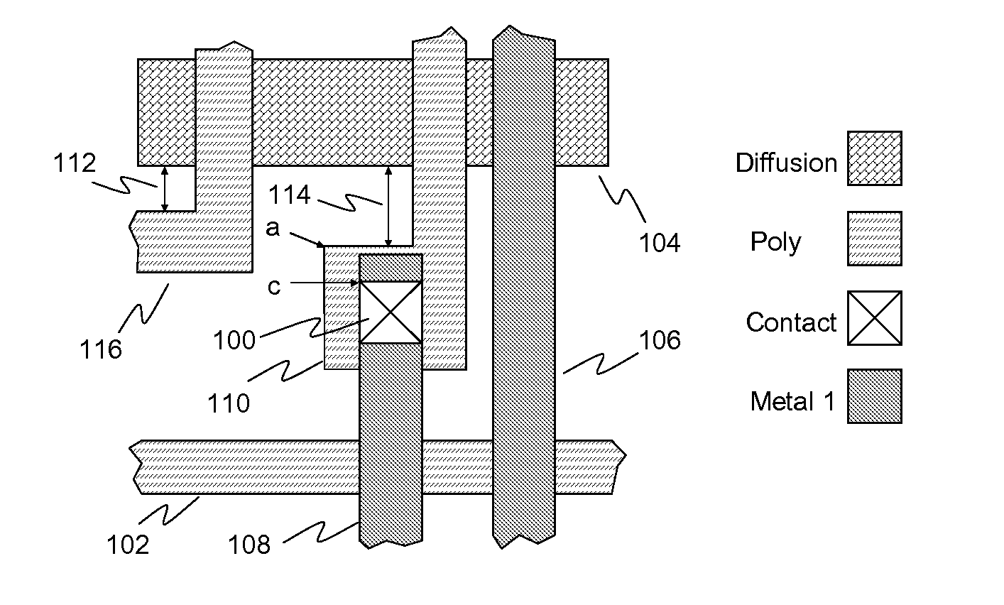
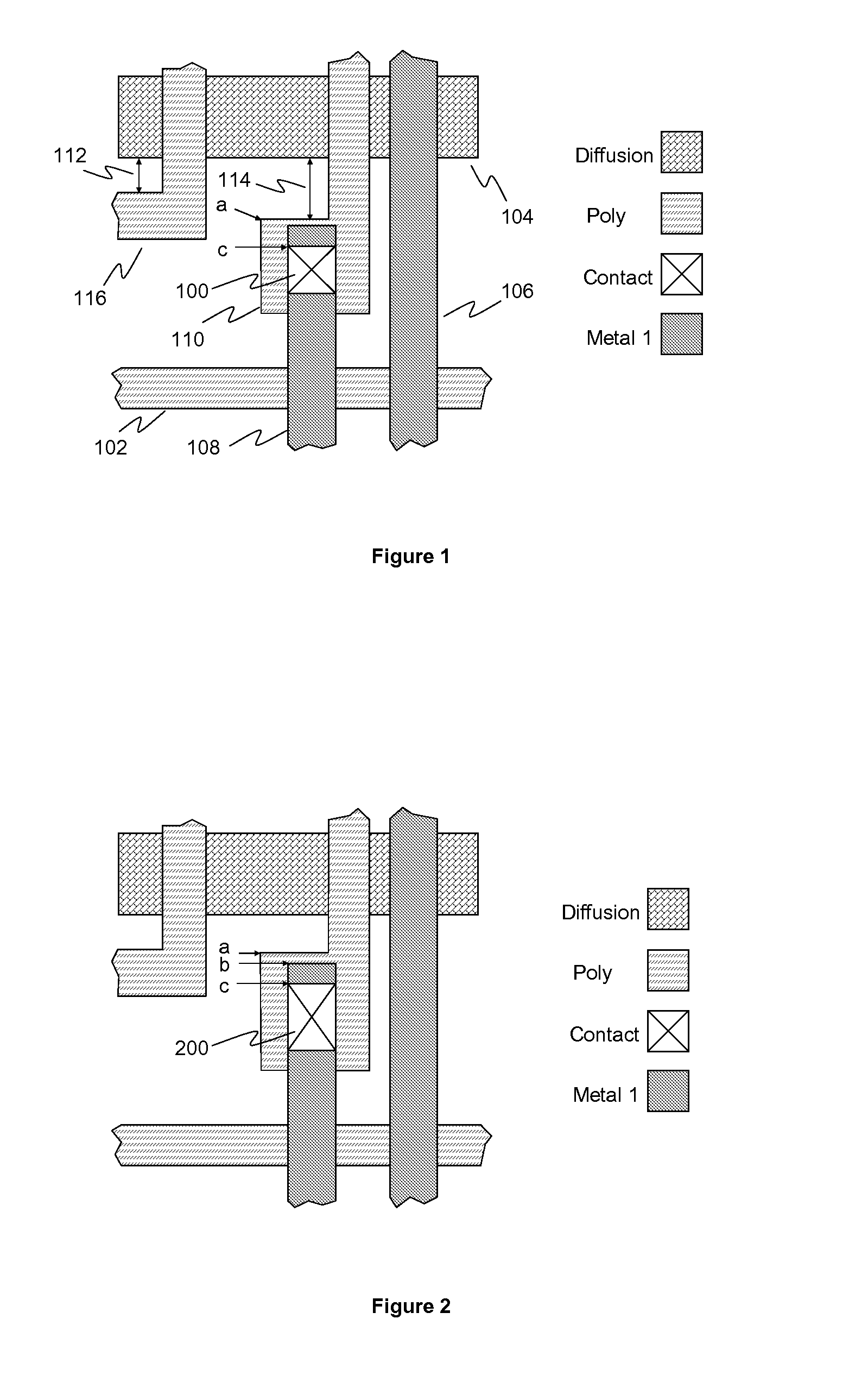
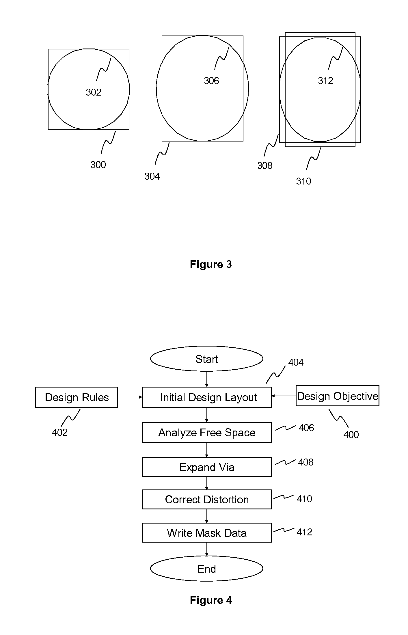
[0035]Some preferred embodiments of the present invention will be described in detail with reference to the related drawings of FIGS. 1-6. Additional embodiments, features and / or advantages of the invention will become apparent from the ensuing description or may be learned by the practice of the invention.

[0036]The methods and apparatus described here are with respect to integrated circuit manufacturing; however, the techniques described here can be applied to manufacturing or design of any device that require pattern transfer of small hole from a polygon database drawing to physical materials using lithographic and / or etch methods. Examples of these include integrated optical devices, microelectromechanical systems (MEMS), gene chips, micromachines, disk drive heads, etc.

[0037]The following description includes the best mode presently contemplated for carrying out the invention. This description is not to be taken in a limiting sense, but is made merely for describing the general ...


PUM


Abstract

A method and system for improving the yield of integrated devices is invented by adaptively selecting contact and via sizes. According to this invention, the drawn size of via holes in a design layout is selected based on its neighboring layout geometries. The invention comprises identifying the minimal space required for placing a via; analyzing available free space for potential via size increase; identifying the proximity configuration of the via with other vias on the via layer; selecting an appropriate via size based on the free space and proximity configuration to create an improved design layout; and fabricate the new layout with model based proximity correction such that vias of a plurality of sizes are reproduced on silicon within predetermined tolerances.

Description

CROSS REFERENCE TO RELATED APPLICATIONS[0001]This application is a continuation of and claims priority to U.S. patent application Ser. No. 11 / 164,106 filed on Nov. 10, 2005.[0002]The application referenced above is incorporated herein by reference in its entirety.FIELD OF THE INVENTION[0003]The present invention relates generally to the manufacturing of integrated devices and more particularly to methods and system for optimizing their design layout for yield improvement.BACKGROUND OF THE INVENTION[0004]An integrated circuit chip is fabricated according to a design layout. A typical design layout has polygonal shapes arranged in different layers, where each layer is associated with a certain step in manufacturing process. A modern integrated circuit chip has many layers comprising active devices, interconnecting conductors, and via layers. The active devices are responsible for amplification or switching while interconnect and vias are responsible for wiring the active devices toget...

Claims


Application Information

Patent Timeline
Patent Type & Authority Applications(United States)
IPC IPC(8): G06F17/50
CPCG06F17/5077G06F2217/12Y02P90/265G06F30/394G06F2119/18Y02P90/02
Inventor QIAN, QI-DE
Owner QI DE QTAN
Why Eureka
Try Eureka