Semiconductor memory device

a memory device and semiconductor technology, applied in the direction of information storage, static storage, digital storage, etc., can solve the problems of disadvantageous increase in the cell area of the dual-port sram cell b>209/b>, disadvantageous increase in the space for arranging the bit lines blb>1/b>, wlb>1/b> and wlb>2/b>, etc., to suppress the increase in

Active Publication Date: 2006-05-30
SEMICON COMPONENTS IND LLC
View PDF12 Cites 18 Cited by
  • Summary
  • Abstract
  • Description
  • Claims
  • Application Information

AI Technical Summary

Benefits of technology

[0013]The present invention has been proposed in order to solve the aforementioned problems, and an object of the present invention is to provide a semiconductor memory device capable of improving the operating speed while suppressing size increase.

Problems solved by technology

Thus, the access from the second system enters the wait state during the access from the first system, and hence it is disadvantageously difficult to improve the operating speed in the semiconductor memory device employing the exemplary conventional single-port SRAM cell 206 shown in FIG. 15.
Thus, the space for arranging the bit lines BL1, / BL1, BL2 and / BL2 and the word lines WL1 and WL2 is disadvantageously increased.
Thus, the cell area of the dual-port SRAM cell 209 is disadvantageously increased as compared with the single-port SRAM cell 206 due to the increased number of the transistors.
Therefore, the space for arranging the bit lines BL1, / BL1, BL2 and / BL2 and the word lines WL1 and WL2 as well as the cell area are increased in the conventional dual-port SRAM cell 209 shown in FIG. 16, to disadvantageously increase the size of the semiconductor memory device.
Thus, the size of the semiconductor memory device constituted of only dual-port SRAM cells must disadvantageously be increased in order to improve the operating speed thereof.

Method used


Image

  • Semiconductor memory device
  • Semiconductor memory device
  • Semiconductor memory device

Examples


first embodiment

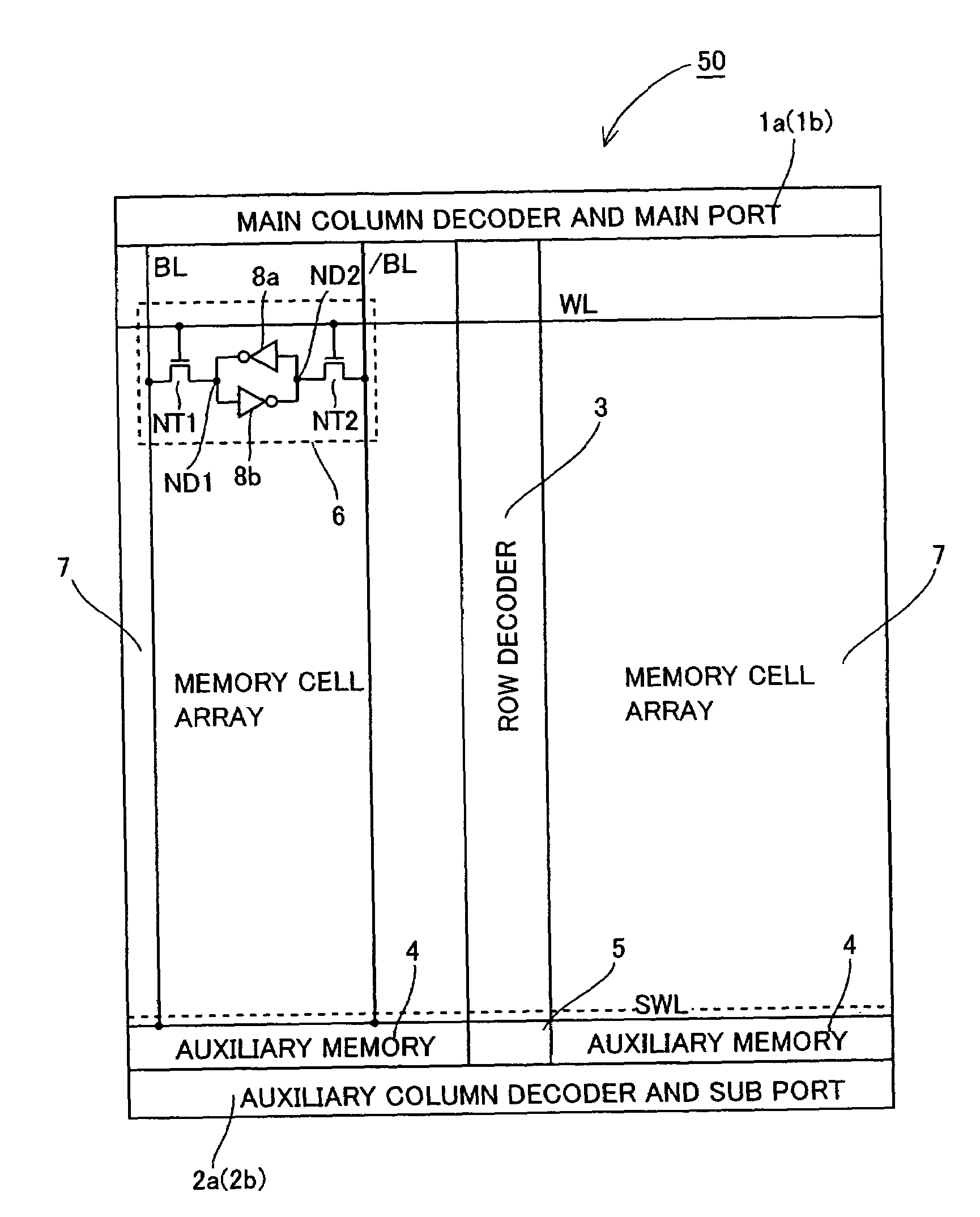
[0058]The structure of a semiconductor memory device 50 according to a first embodiment of the present invention is described with reference to FIGS. 1 to 6.

[0059]As shown in FIG. 1, the semiconductor memory device 50 according to the first embodiment of the present invention comprises a main column decoder 1a and an auxiliary column decoder 2a for selecting column addresses as well as a row decoder 3 for selecting row addresses. The main column decoder 1a includes a main port 1b for externally inputting / outputting data. The auxiliary column decoder 2a includes a sub port 2b for externally outputting data. The row decoder 3 is provided on the central portion of the semiconductor memory device 50. A transfer signal generation circuit 5 for supplying a transfer signal TF etc. to auxiliary memories 4 described later is provided on an end of the row decoder 3 closer to the auxiliary column decoder 2a. Two memory cell arrays 7 formed with single-port SRAM cells 6 etc. are provided on bot...

second embodiment

[0092]As shown in FIG. 8, a card reader 150 including an SRAM-IP 155 according to a second embodiment of the present invention is connected to a personal computer 152 through a USB cable 151. This personal computer 152 comprises a hard disk 152a for storing data. The card reader 150 is so constituted that a flash card 153 serving as a data recording medium can be mounted thereon. The card reader 150 comprises a microcomputer 154 and the SRAM-IP (intellectual property) 155. The term “SRAM-IP” indicates a functional block of an SRAM built into a chip. This SRAM-IP 155 has a function of temporarily stocking data output from the hard disk 152a of the personal computer 152 and the flash card 153. The details of the SRAM-IP 155 are described later. The microcomputer 154 is provided in order to control data transfer between the hard disk 152a of the personal computer 152 and the flash card 153 and the SRAM-IP 155.

[0093]In operation, the card reader 150 including the SRAM-IP 155 according t...

third embodiment

[0115]The structure of a semiconductor memory device (SRAM-IP) 165 according to a third embodiment of the present invention is described with reference to FIG. 14. According to the third embodiment, the semiconductor memory device (SRAM-IP) 165 has access means for writing simultaneously received data of prescribed capacity in different addresses in different cycles every byte unit (8 bits), dissimilarly to the aforementioned second embodiment.

[0116]In the structure of the SRAM-IP 165 according to the third embodiment, four (four-byte) input / output circuit parts 110 for inputting and outputting data are connected to a second column decoder 102b of the SRAM-IP 165, as shown in FIG. 14. FIG. 14 shows only the structure of one (one-byte) input / output circuit part 110, for simplifying the illustration. This input / output circuit part 110 is an example of the “access means” or the “access circuit part” in the present invention. Each input / output circuit part 110 includes eight circuit par...


PUM


Abstract

A semiconductor memory device capable of improving the operating speed while suppressing size increase is provided. This semiconductor device comprises a plurality of word lines and a plurality of bit lines arranged to intersect with each other, a single-port SRAM cell, connected to the bit lines and the word lines, having a single port for inputting / outputting data, a first row decoder and a second row decoder connected to the word lines for selecting a row address and a first column decoder and a second column decoder connected to the bit lines for selecting a column address, while each word line is divided into a plurality of local word lines.

Description

BACKGROUND OF THE INVENTION[0001]1. Field of the Invention[0002]The present invention relates to a semiconductor memory device, and more particularly, it relates to a semiconductor memory device including SRAM (static random access memory) cells.[0003]2. Description of the Background Art[0004]A semiconductor memory device employing a single-port SRAM cell having a single port for inputting / outputting data is known in general. FIG. 15 is a circuit diagram showing an exemplary conventional single-port SRAM cell 206. Referring to FIG. 15, the exemplary conventional single-port SRAM cell 206 is constituted of six transistors in total, i.e., four n-channel transistors NT201, NT202, NT206 and NT207 and two p-channel transistors PT201 and PT202.[0005]In operation, a semiconductor memory device employing the exemplary conventional single-port SRAM cell 206 shown in FIG. 15 holds the potential of a word line WL at a low level in an initial state. Thus, the semiconductor memory device holds t...

Claims


Application Information

Patent Timeline
Patent Type & Authority Patents(United States)
IPC IPC(8): G11C8/00G11C11/00G11C8/16G11C11/412
CPCG11C11/412G11C8/16
Inventor YAMADA, KOUICHI
Owner SEMICON COMPONENTS IND LLC
Why Eureka
Try Eureka