Method of producing circuit board by additive method, and circuit board and multilayer circuit board obtained by the method

A multi-layer circuit board, circuit board technology, applied in the direction of multi-layer circuit manufacturing, three-dimensional rigid printed circuit board, circuit, etc., can solve the problems of electrical conductivity, deterioration of line strength, complicated manufacturing process and other problems

Inactive Publication Date: 2011-02-23
PANASONIC CORP
View PDF5 Cites 15 Cited by
  • Summary
  • Abstract
  • Description
  • Claims
  • Application Information

AI Technical Summary

Problems solved by technology

However, this method requires preparing two photosensitive resin layers with different solvent solubility, developing them with two solvents, and dissolving the second photosensitive resin with an alkaline solution after adsorbing the catalyst, so the manufacturing process is very complicated.
[0015] Preparing circuits with narrow line widths and line spacings by using the circuit forming method as described above also causes the following problems: Specifically, reducing the line widths and line spacings of the circuits leads to deterioration of line strength
[0020] Resin smear 305 remaining on bottom of IVH 304 may cause conductivity annoyance

Method used


Image

  • Method of producing circuit board by additive method, and circuit board and multilayer circuit board obtained by the method
  • Method of producing circuit board by additive method, and circuit board and multilayer circuit board obtained by the method
  • Method of producing circuit board by additive method, and circuit board and multilayer circuit board obtained by the method

Examples


no. 1 example

[0049] First Embodiment (Method of Manufacturing Circuit Board by Using Expandable Resin Film)

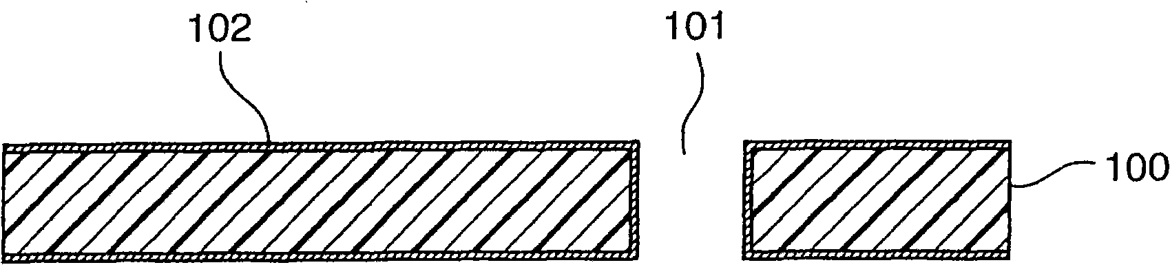
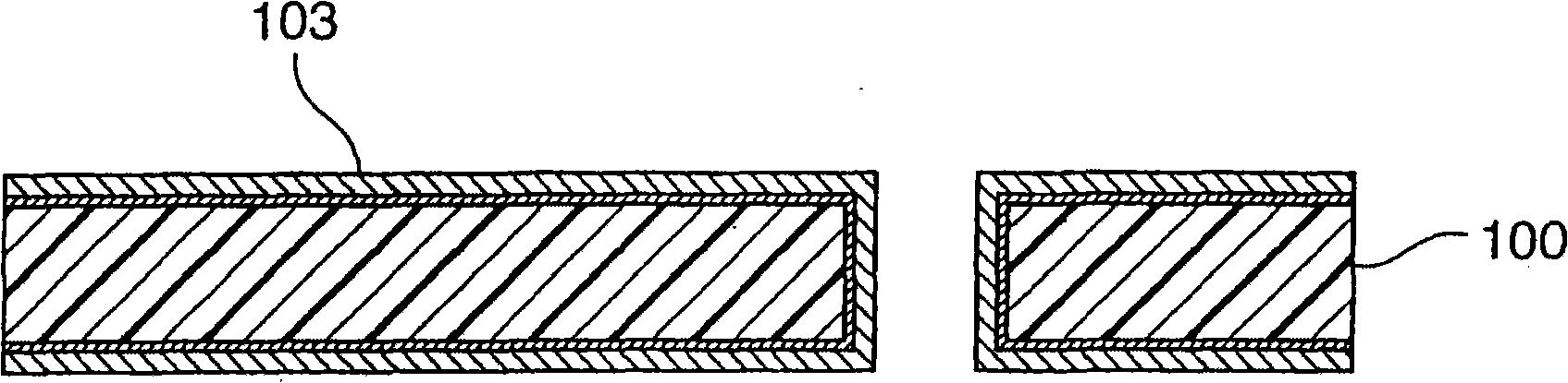
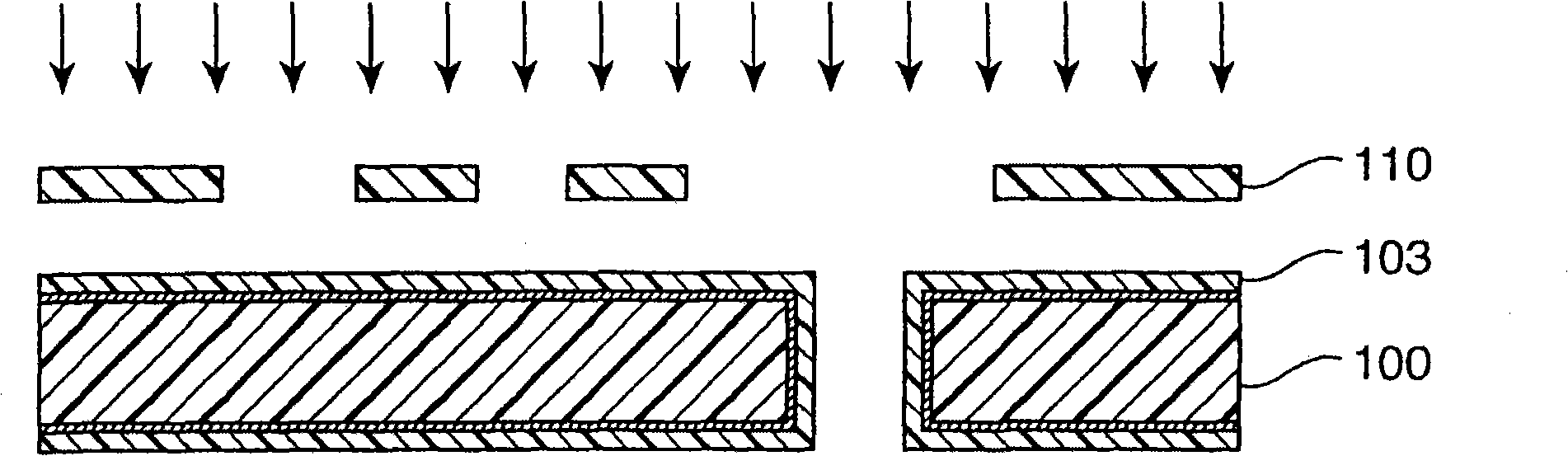
[0050] The method of manufacturing the circuit board in this embodiment will be described with reference to the accompanying drawings. Figures 5A to 5E is a schematic cross-sectional view illustrating the steps of the method of manufacturing the circuit board in the first embodiment. exist Figures 5A to 5E 2, an expandable resin film; 3, a circuit groove; 4, a through hole passing through a part of the circuit groove 3; 5, a plating catalyst; and 6, an electroless plating film. In the manufacturing method of this embodiment, as Figure 5A As shown, the expandable resin film 2 is first formed on the surface of the insulating substrate 1 . The swellable resin film means a resin film that is easily separated from the substrate surface by swelling with a special liquid.

[0051] Various organic substrates used in manufacturing circuit boards can be used as the insulating substrat...

example 1

[0090] A styrene-butadiene copolymer (SBR) film with a thickness of 2 μm was formed on the surface of an epoxy resin substrate (R1766 manufactured by Matsushita Electric Works Co., Ltd.) having a thickness of 100 μm. By coating a suspension of styrene-butadiene copolymer (SBR) in methyl ethyl ketone (MEK) (manufactured by Zeon Corporation, acid equivalent: 600, particle diameter: 200 nm, solid matter: 15%) It was spread on the main surface of an epoxy resin substrate, and the resulting coating film was dried at 80° C. for 30 minutes to form a film.

[0091] A groove having an approximately rectangular cross-section with a width of 20 μm and a depth of 30 μm was formed on the film-formed epoxy resin substrate by laser processing. Model 5330 manufactured by ESI equipped with a UV-YAG laser was used for this laser processing.

[0092] The laser-processed epoxy substrate was then dipped in a detergent conditioner (pH<1 surfactant solution, C / N3320 manufactured by Rohm and Haas El...

no. 2 example

[0100] Second Embodiment (Method of Forming Local Reinforcement Structure in Fine Wiring)

[0101] By carrying out the method of manufacturing a circuit board described in the first embodiment, a local reinforcement structure to be described below can be formed for local reinforcement of a circuit.

[0102] The method of manufacturing the circuit board in this embodiment will be described with specific reference to the accompanying drawings. To prevent repetition, only those common to the description of the first embodiment will be briefly described.

[0103] 7A to 7E are schematic cross-sectional views respectively illustrating the steps of the method of manufacturing the circuit board in the second embodiment.

[0104] In the manufacturing method of this embodiment, as Figure 7A As shown, the resin film 12 is first formed on the surface of the insulating substrate 1 .

[0105] Various organic substrates similar to those described in the first embodiment can be used as ...


PUM


Abstract

The method of producing a multilayer circuit board includes a film-forming step of forming a swellable resin film on the surface of an insulative substrate, a circuit groove-forming step of forming circuit grooves having a depth equal to or greater than the thickness of the swellable resin film on the external surface of the swellable resin film, a catalyst-depositing step of depositing a platingcatalyst on the surface of the circuit grooves and the surface of the swellable resin film, a film-separating step of swelling the swellable resin film with a particular liquid and then separating the swollen resin film, and a plating processing step of forming an electrolessly plated film only in the region where the plating catalyst or the plating catalyst formed from the plating catalyst precursor remains unseparated after separation of the swellable resin film.

Description

technical field [0001] The present invention relates to a method for manufacturing a circuit board by an additive method, and a circuit board and a multilayer circuit board obtained by the method. Background technique [0002] Recently, there has been a rapid increase in the functionality of electrical equipment including portable information systems such as cell phones, computers and peripherals thereof, various information appliances, and the like. Along with this trend, there has been an increase in demand for increasing circuit density on circuit boards used in these electrical devices. To increase the density of such circuits, there is a need for a method of accurately fabricating circuits with narrower line widths and line spacings. Problems such as shorts and migrations between lines are often found in high-density wiring circuits. In addition, the narrow width of the wiring leads to deterioration of the mechanical strength of the wiring, making the resulting circui...

Claims


Application Information

Patent Timeline
Patent Type & Authority Applications(China)
IPC IPC(8): H05K3/10H05K3/46H05K3/18H05K1/02H05K1/16
CPCH05K2203/0565H05K1/111H05K3/465H05K2201/09845H05K3/4647H05K1/0206H05K1/0284H01L2224/48227H05K2201/09736H05K2203/0108H05K1/162H05K3/0032H01L2924/15311H05K1/0269H05K3/184H05K3/4661H05K3/107H05K2203/161H05K2201/2072H05K1/02H05K3/10H05K3/18H05K3/46
Inventor 吉冈慎悟藤原弘明
Owner PANASONIC CORP
Why Eureka
Try Eureka