Wafer cutting tool and method for cutting wafer by using same

A technology for cutting tools and wafers, used in manufacturing tools, work accessories, stone processing equipment, etc., can solve the problems of difficulty in determining the position of the cutting line, inaccurate cutting, etc., to achieve diversified motion trajectories, low cost, and a wide range of applications Effect

Active Publication Date: 2013-06-12
SEMICON MFG INT (SHANGHAI) CORP +1
View PDF0 Cites 0 Cited by
  • Summary
  • Abstract
  • Description
  • Claims
  • Application Information

AI Technical Summary

Problems solved by technology

[0009] The problem solved by the present invention is to provide a wafer cutting tool and a method for cutting a wafer using the tool, which solves the problem of determining the position of the cutting line encountered when extracting the region of interest from the wafer during the chip testing process Difficulty causing the problem of inaccurate cutting

Method used


Image

  • Wafer cutting tool and method for cutting wafer by using same
  • Wafer cutting tool and method for cutting wafer by using same
  • Wafer cutting tool and method for cutting wafer by using same

Examples


Embodiment Construction

[0037] The present invention will be further described below in conjunction with specific embodiments and accompanying drawings, but the protection scope of the present invention should not be limited thereby.

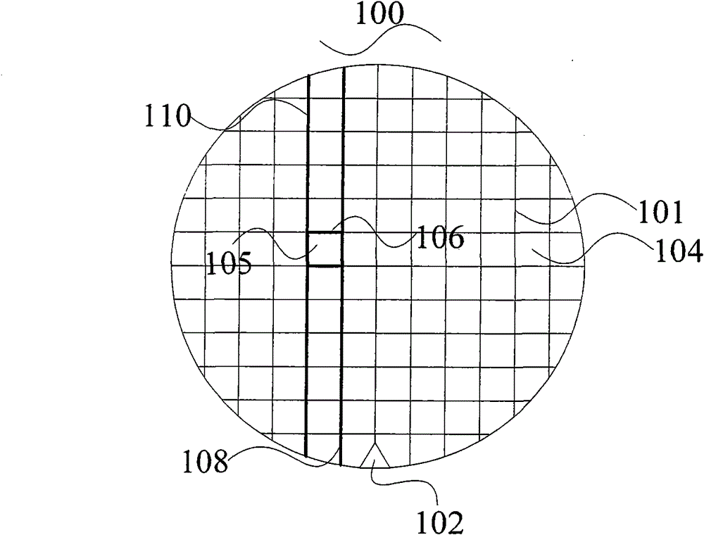
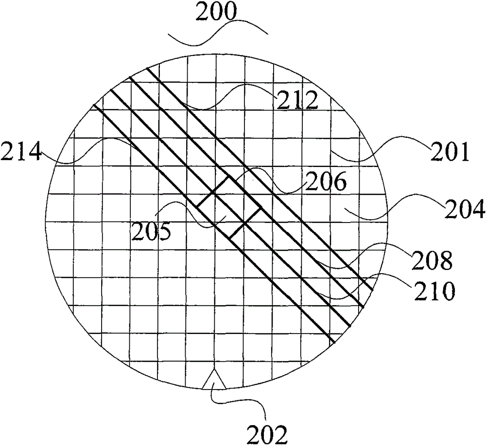
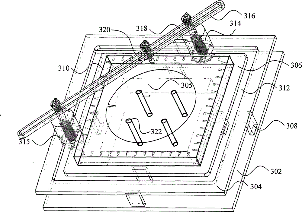
[0038] image 3 It is a schematic structural diagram of a wafer cutting tool according to an embodiment of the present invention. The wafer cutting tool includes: a tool base 302; a peripheral support 304 and a wafer carrier 306, which are respectively connected to the tool base 302 through pillars 308 , at least one of the peripheral bracket 304 and the wafer carrier 306 has a scale 310 around it, the peripheral bracket 304 surrounds the outer side of the wafer carrier 306, and leaves a gap between the wafer carrier 306 , as a slider track 312; sliders 314, 315 can slide along the slider track 312; a slider 316 has an inner groove 318, and the inner groove 318 is sleeved on the sliders 314, 315, so that the Slide bar 316 can slide on the line direction of two slide blo...


PUM


Abstract

The invention provides a wafer cutting tool. The wafer cutting tool comprises a peripheral bracket, a wafer bearing table, slide blocks, a slide rod and a cutter, wherein scales are carved on the circumference of at least one of the peripheral bracket and the wafer bearing table; the peripheral bracket surrounds the outer side of the wafer bearing table; a gap is reserved between the peripheral bracket and the wafer bearing table and serves as a slide block track; the slide blocks can slide along the slide block track; an inner groove is arranged in the slide rod and is sleeved on the slide block, so that the slide rod can slide in the connection line direction of the two slide blocks, and the slide rod has the length that each position of a wafer can be cut; the cutter is positioned between the two slide blocks on the slide rod and can slide along the inner groove of the slide rod to cut the wafer; and at least one of the slide rod and the cutter can be adjusted in the height direction. Correspondingly, the invention also provides a method for cutting the wafer. A cutting line position of an interested area on the wafer can be quickly and precisely determined and cut by the wafercutting tool.

Description

technical field [0001] The invention relates to the technical field of semiconductor manufacturing, in particular to a wafer cutting tool and a method for cutting wafers using the tool. Background technique [0002] In the semiconductor manufacturing process, in order to accurately locate the rotation direction of the wafer, a positioning notch (notch) of a wafer is usually defined on the outer edge of the wafer in the <110> direction, and the positioning notch is aligned with each chip in the wafer. (die) corresponds to the orientation. [0003] However, with the development of manufacturing processes applied to silicon with a feature size below 90nm, more new process technologies are introduced into the CMOS process to increase the performance of semiconductor devices. Wherein, the direction of the chip is changed from the original <110> direction to the <100> direction, and the direction of the corresponding wafer positioning notch is also changed from ...

Claims


Application Information

Patent Timeline
Patent Type & Authority Patents(China)
IPC IPC(8): B28D5/04B28D7/00B28D7/04H01L21/304
Inventor 陈险峰葛挺锋娄晓祺邹丽君
Owner SEMICON MFG INT (SHANGHAI) CORP
Why Eureka
Try Eureka