Failure analysis method of gate oxide

A gate oxide layer and failure analysis technology, which is applied in the field of semiconductor manufacturing, can solve the problems of complex detection process, failure detection results, long detection cycle, etc., and achieve the effects of improving success rate, saving time, and easy control

Active Publication Date: 2011-03-30
SEMICON MFG INT (SHANGHAI) CORP
View PDF0 Cites 19 Cited by
  • Summary
  • Abstract
  • Description
  • Claims
  • Application Information

AI Technical Summary

Problems solved by technology

[0012] In order to solve a series of problems such as the failure analysis method for the gate oxide layer in the prior art, the detection process is extremely complicated, the detection period is relatively long, failure detection results are easy to be generated, and the detection cost is high. Methods for Failure Analysis of Oxide Layers

Method used


Image

  • Failure analysis method of gate oxide
  • Failure analysis method of gate oxide
  • Failure analysis method of gate oxide

Examples


Embodiment Construction

[0036] In order to make the content of the present invention clearer and easier to understand, the content of the present invention will be described in detail below in conjunction with specific embodiments and accompanying drawings.

[0037] The method for performing failure analysis on the gate oxide layer in this embodiment includes:

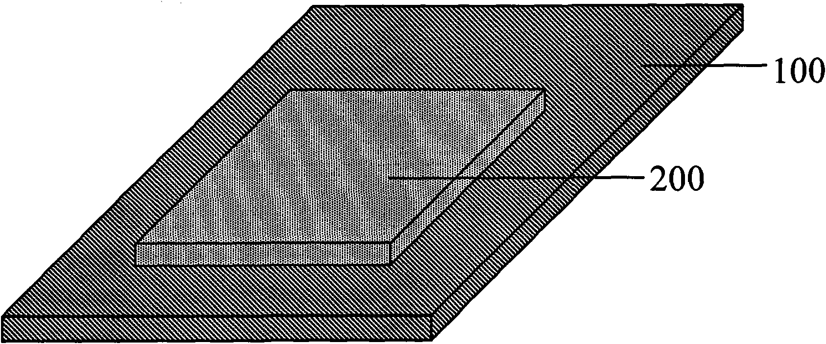
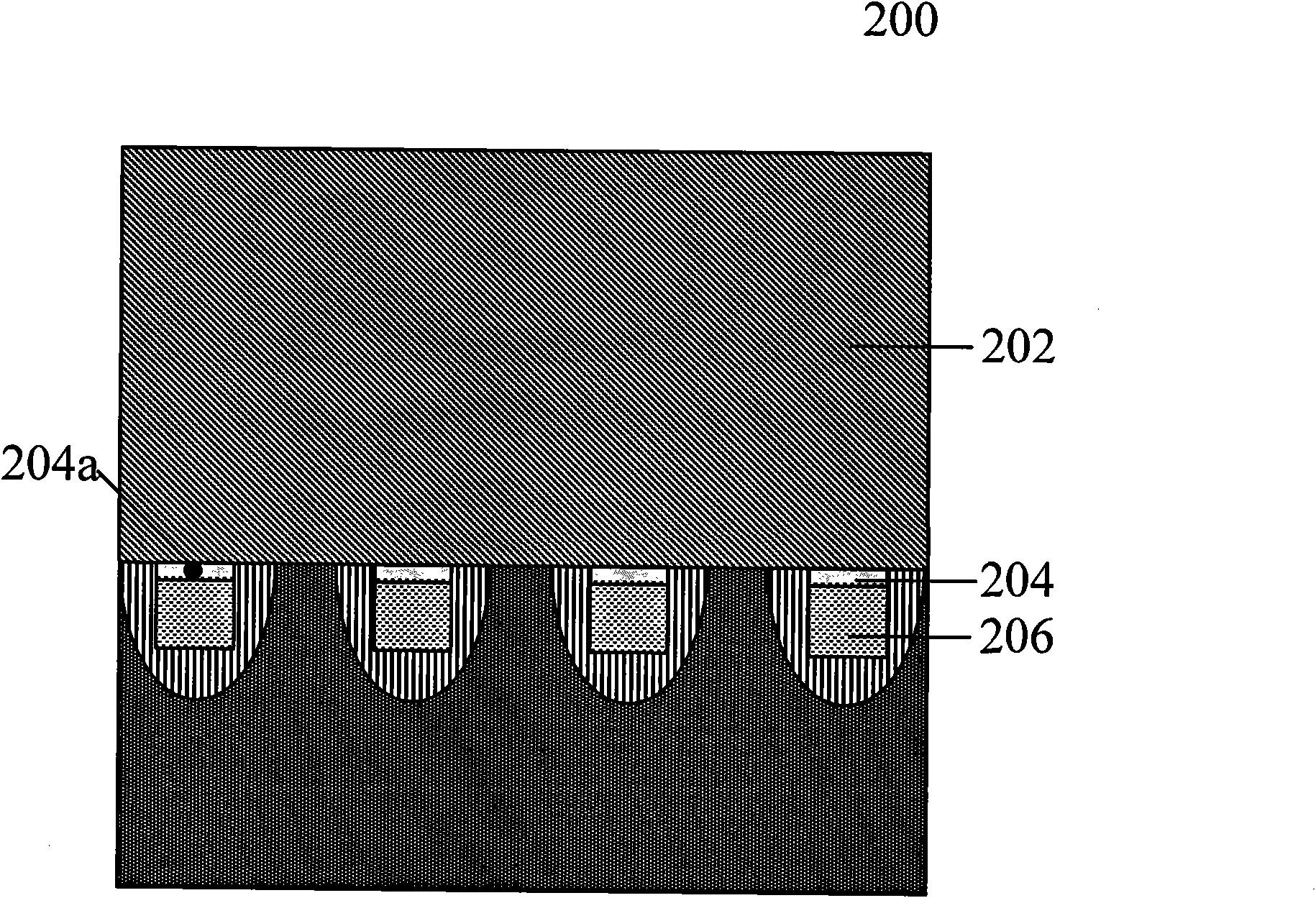
[0038] First, the invalid wafer is pasted upside down on the substrate with thermal gel, and the invalid wafer includes the substrate and the gate oxide layer on the substrate;

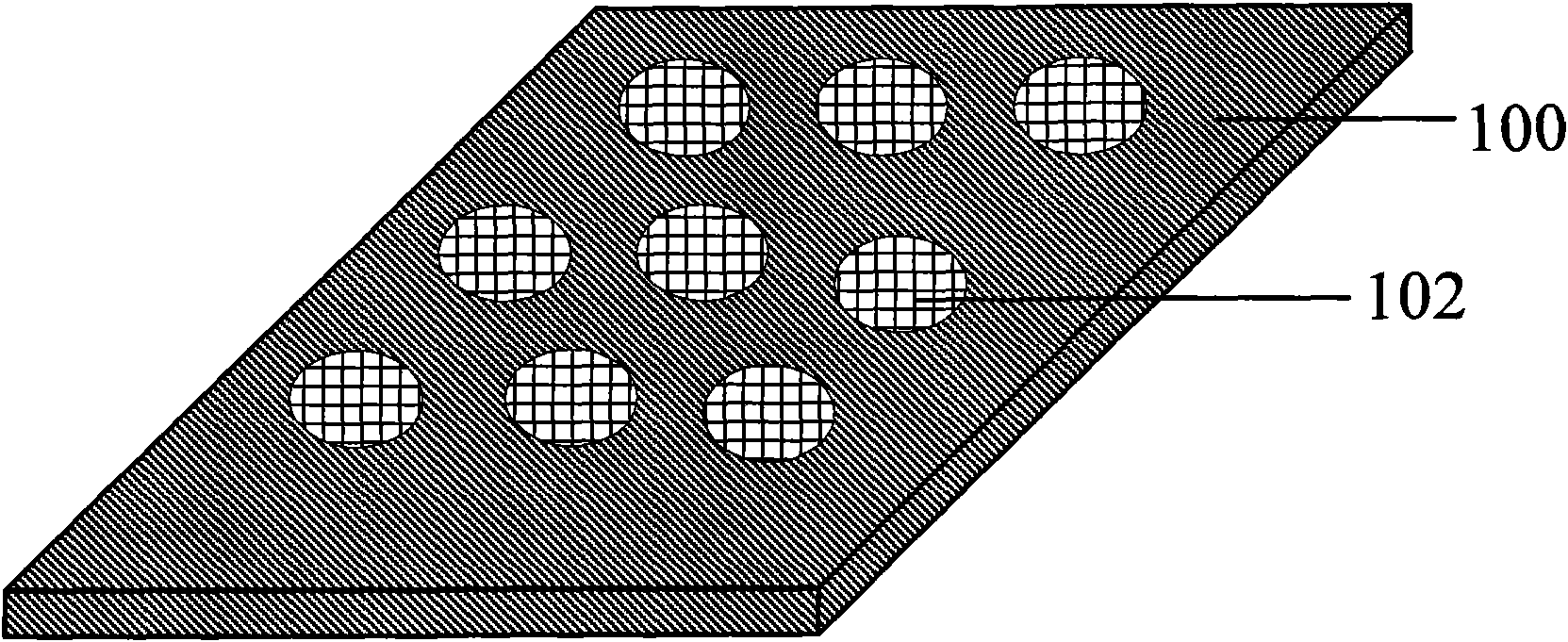
[0039] Preferably, in order to make the thermal gel evenly coated and to have good adhesion between the failed wafer and the substrate, the thermal gel is divided into a plurality of uniform thermal gel points, which are evenly dropped on the substrate in an array;

[0040] Preferably, the invalid wafer is pasted upside down on the substrate with thermal gel, further comprising: applying uniform pressure to the substrate and the wafer and heating it, so that the two ...


PUM

PropertyMeasurementUnit
thicknessaaaaaaaaaa

Abstract

The invention provides a failure analysis method of a gate oxide, which ensures that problems of extremely complicated detection process of a failure chip, relatively long detection period, easy occurrence of failed detection results, higher detection cost and the like in the prior art can be solved. The failure analysis method comprises the following steps: pasting the failure chip reversely on a substrate by hot gel, wherein, the failure chip comprises a substrate and the gate oxide on the substrate; grinding the substrate of the failure chip to certain thickness or fully removing the substrate; soaking the surface of the chip with alkaline solution; and observing the failure chip, wherein, the gate oxide is defective when a control gate is damaged, and the gate oxide is intact when the control gate is undamaged. The detection method of the failure chip has the advantages of simplicity, shorter time consumption, less possibility of failure and lower cost.

Description

technical field [0001] The invention relates to the technical field of semiconductor manufacturing, and more specifically relates to a method for performing failure analysis on gate oxide layers when manufacturing semiconductor devices. Background technique [0002] With the development of semiconductor technology, the size of components in semiconductor devices (such as chips) is continuously shrinking, and the failure cases caused by the quality problems of the gate oxide layer (GOX) are also increasing. Therefore, failure analysis of the gate oxide layer is becoming more and more important. [0003] An existing method for detecting gate oxide failure analysis includes: [0004] Grinding failed samples down to a layer that can be pinpointed; [0005] Mark known failure locations with a Focused Ion Beam (FIB) machine; [0006] Continue to grind the sample to the polysilicon gate (Poly), this step needs to use the scanning microscope to observe the grinding treatment degr...

Claims


Application Information

Patent Timeline
Patent Type & Authority Applications(China)
IPC IPC(8): H01L21/66G01N1/32
Inventor 孙静钱峰
Owner SEMICON MFG INT (SHANGHAI) CORP
Why Eureka
Try Eureka