STI forming method

A technology of mask pattern and hard mask layer, which is applied in the field of STI formation, can solve the problem of etching barrier layer falling off, and achieve the effect of reducing the possibility of falling off and high planarization efficiency

Inactive Publication Date: 2011-03-30
SEMICON MFG INT (SHANGHAI) CORP +1
View PDF1 Cites 5 Cited by
  • Summary
  • Abstract
  • Description
  • Claims
  • Application Information

AI Technical Summary

Problems solved by technology

[0005] The etch stop layer described in the above STI formation method is usually a stacked structure of a polysilicon layer and a silicon nitride layer. It is found in the STI manufacturing process that when t

Method used


Image

  • STI forming method
  • STI forming method
  • STI forming method

Examples


Embodiment Construction

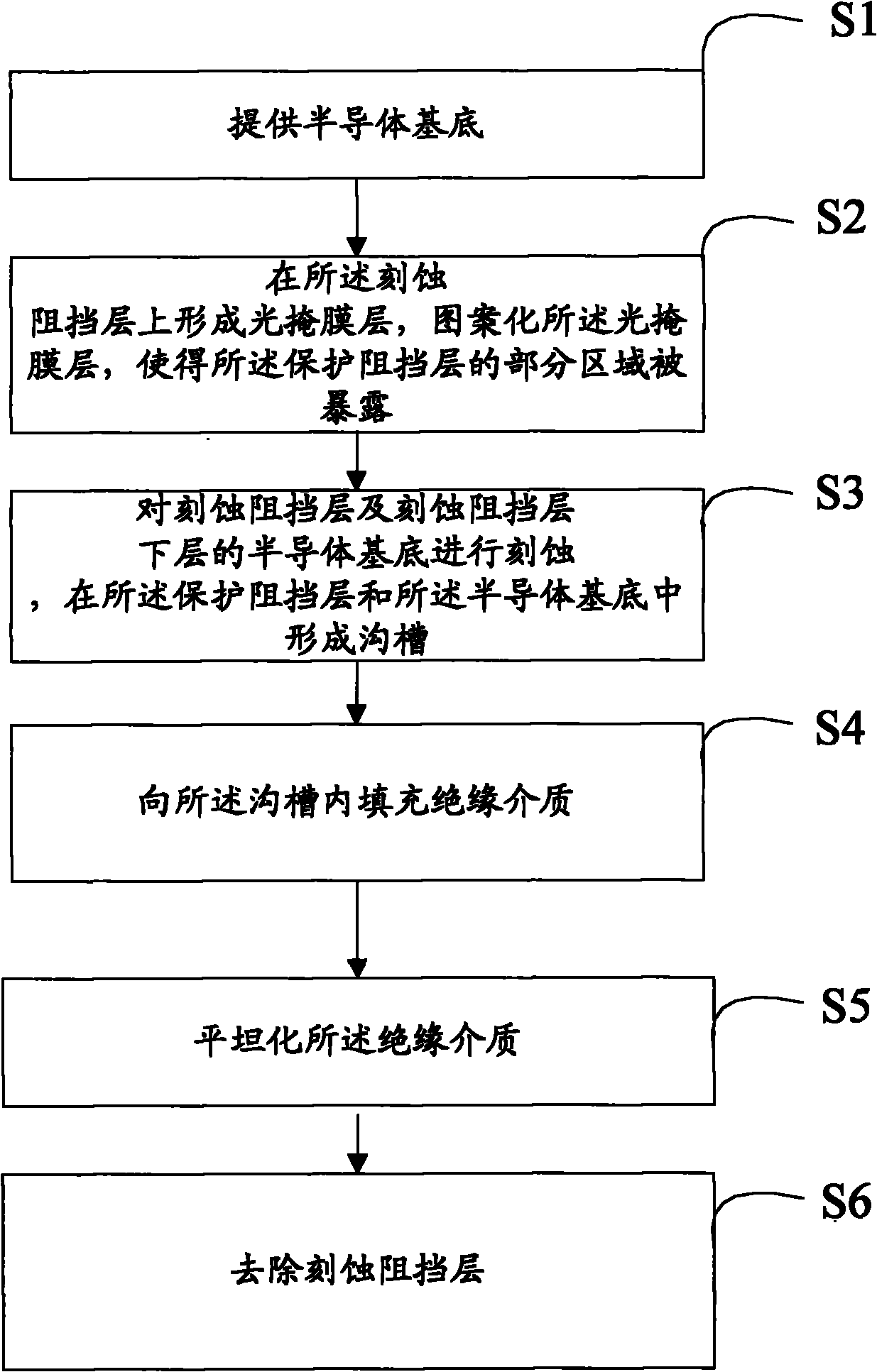
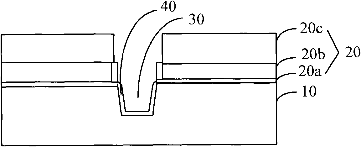
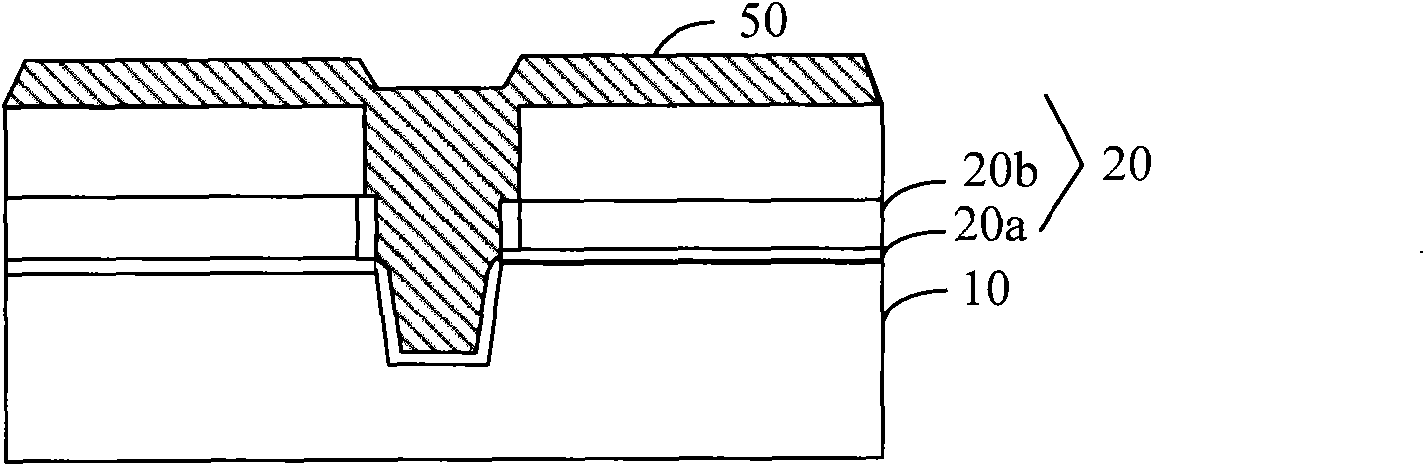
[0026] It can be seen from the background technology that in the formation process of STI, a layer of etch stop layer is usually formed on the semiconductor substrate; then a mask layer with an opening pattern is formed on the etch stop layer; and then etched at the opening of the mask layer A trench is formed in the semiconductor substrate and the etch barrier layer; then an insulating medium is filled into the trench; then the insulating medium is planarized; finally, the etch barrier layer is removed to form an STI.

[0027] However, using the existing technology, after etching the semiconductor substrate and forming the groove in the etching barrier layer, it is found that there are some peelings of the etching barrier layer on the substrate. The inventor of the present invention thinks after research: The stacked structure of silicon nitride and polysilicon is used as an etching barrier layer, wherein the silicon nitride layer is used as a hard mask layer of the semiconduc...


PUM


Abstract

The invention provides an STI forming method, comprising the following steps: providing a semiconductor substrate; forming a nitride layer with an atomic layer deposition method on the semiconductor substrate; forming a hard mask on the nitride layer, wherein the nitride layer and the hard mask form an etching barrier layer; etching the hard mask, the nitride layer and the semiconductor substrate so as to form a groove in the hard mask, the nitride layer and the semiconductor substrate; deposing an insulated medium, wherein the insulated medium covers the side wall and the bottom of the groove and the hard mask; planarizing the insulated medium; and removing the nitride layer and the hard mask. The method reduces the possibility that the etching barrier layer is easy to drop off in etching process.

Description

technical field [0001] The invention relates to the technical field of semiconductor manufacturing, in particular to a method for forming an STI. Background technique [0002] As semiconductor technology enters the deep submicron era, in components below 0.13 μm such as CMOS devices, the isolation between NMOS transistors and PMOS transistors is formed by STI (Shallow Trench Isolation) process. [0003] figure 1 It is a flow chart of a manufacturing method of STI in the prior art. refer to figure 1 , the forming method of STI generally includes the steps: S1: providing a semiconductor substrate, specifically, first forming an etching stopper layer on the semiconductor substrate; S2: then forming a photomask layer on the etching stopper layer, and then patterning the A photomask layer, so that a part of the etch barrier layer is exposed; S3: Etch the etch barrier layer and the semiconductor substrate under the etch barrier layer, between the etch barrier layer and the semi...

Claims


Application Information

Patent Timeline
IPC IPC(8): H01L21/762H01L21/318
Inventor 代培刚冯永刚张永兴宋化龙
Owner SEMICON MFG INT (SHANGHAI) CORP
Why Eureka
Try Eureka