

Solid-state imaging device, manufacturing method therefor, and electronic device
A technology of a solid-state imaging device and a manufacturing method, which is applied in the directions of electric solid-state devices, semiconductor devices, radiation control devices, etc., can solve the problems of inability to reduce the size of the device and the reduction of the light-receiving area, and achieve the effect of avoiding the deterioration of pixel characteristics.
Active Publication Date: 2011-04-06
SONY CORP
View PDF12 Cites 14 Cited by
- Summary
- Abstract
- Description
- Claims
- Application Information
AI Technical Summary
Problems solved by technology
However, in this way, although the size of the device can be reduced by adopting a three-dimensional structure, the light receiving area is reduced in the case where wiring and contacts are formed on the light receiving surface
Therefore, in order to maintain the light-receiving area, the pixel area must be increased by the same amount, so the size of the device cannot be reduced
Method used
View moreImage
Smart ImageViewing Examples

Examples
no. 1 example
[0061] First Embodiment: Solid-state imaging device
[0062] 1-1 Overall structure of solid-state imaging device
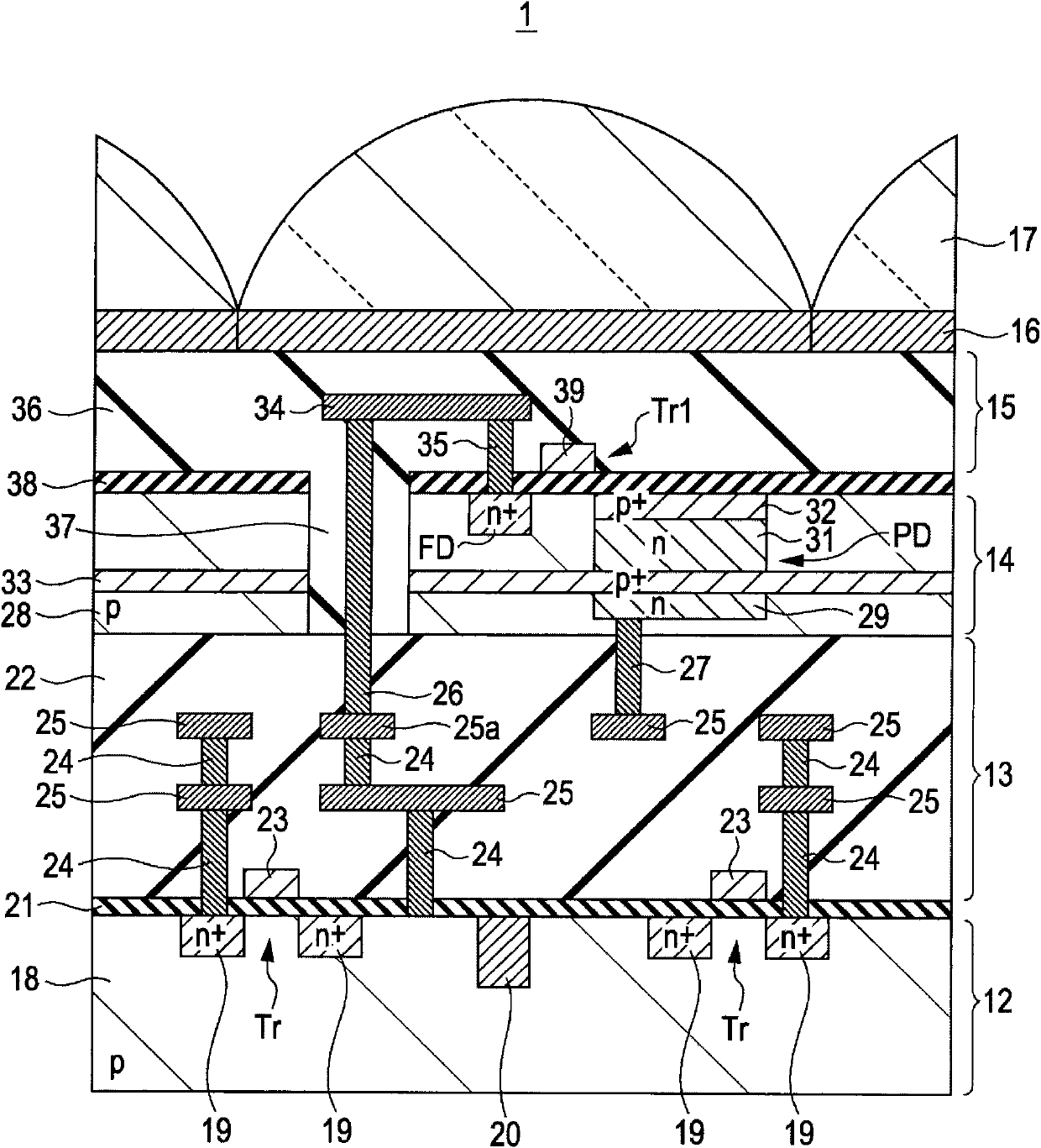
[0063] 1-2 Cross-sectional structure of main parts
[0064] 1-3 Manufacturing method
no. 2 example
[0065] Second Embodiment: Solid-state Imaging Device
[0066] 2-1 Cross-sectional structure of main parts
[0067] 2-2 Manufacturing method
no. 3 example
[0068] Third Embodiment: Solid-state Imaging Device
[0069] 3-1 Cross-sectional structure of main parts
[0070] 3-2 Manufacturing method
Login to View More PUM
 Abstract
The invention relayes to a solid-state imaging device, a manufacturing method therefor, and an electronic device using the solid-state imaging device. The solid-state imaging device includes: a plurality of substrates stacked via a wiring layer or an insulation layer; a light sensing section that is formed in a substrate, of the plurality of substrates, disposed on a light incident side and that generates a signal charge in accordance with an amount of received light; and a contact portion that is connected to a non-light incident-surface side of the substrate in which the light sensing section is formed and that supplies a desired voltage to the substrate from a wire in a wiring layer disposed on a non-light incident side of the substrate. The solid-state imaging device could reduce the size of the solid-state imaging device without reducing the light receiving area.
Description
[0001] Cross References to Related Applications [0002] The present application contains subject matter related to the disclosure of Japanese Priority Patent Application JP2009-198118 filed in the Japan Patent Office on Aug. 28, 2009, the entire content of which is hereby incorporated by reference. technical field [0003] The present invention relates to a solid-state imaging device, and more particularly to a solid-state imaging device formed by stacking a plurality of substrates and a method of manufacturing the solid-state imaging device. The present invention also relates to an electronic device using the solid-state imaging device. Background technique [0004] Solid-state imaging devices are roughly divided into charge-transport solid-state imaging devices represented by Charge Coupled Device (CCD) image sensors and amplification devices represented by Complementary Metal Oxide Semiconductor (Complementary Metal Oxide Semiconductor, CMOS) image sensors. solid-state ...
Claims
Login to View More Application Information
Patent Timeline
 Patent Type & AuthorityApplications(China)
IPC IPC(8): H01L27/146H01L27/148H04N5/335H04N5/374H04N5/341H04N5/225H04N25/00
CPCH01L27/14692H01L27/14609H01L27/14887H01L27/1469H01L27/14683H01L27/14689H01L27/14636H01L27/14634H01L27/14656H01L27/1464H01L27/146H04N25/00
Inventor松沼健司
OwnerSONY CORP