Terminal of power semiconductor and manufacturing method of terminal

A technology for power semiconductors and manufacturing methods, which is applied in the fields of semiconductor devices, semiconductor/solid-state device manufacturing, electrical components, etc. The effect of early breakdown, uniform distribution, and uniform distribution of the electric field

Active Publication Date: 2012-09-05
BYD SEMICON CO LTD
View PDF0 Cites 0 Cited by
  • Summary
  • Abstract
  • Description
  • Claims
  • Application Information

AI Technical Summary

Problems solved by technology

The analysis shows that the simultaneous effect of decreasing junction depth and decreasing doping concentration will cause the resistance of JTE to increase rapidly outward along the main junction, which is not conducive to the effective transfer of potential, resulting in the sharing of too high potential near the main junction, and the electric field If it is too high, it will break down prematurely and fail to achieve the purpose of effective protection

Method used


Image

  • Terminal of power semiconductor and manufacturing method of terminal
  • Terminal of power semiconductor and manufacturing method of terminal
  • Terminal of power semiconductor and manufacturing method of terminal

Examples


Embodiment 1

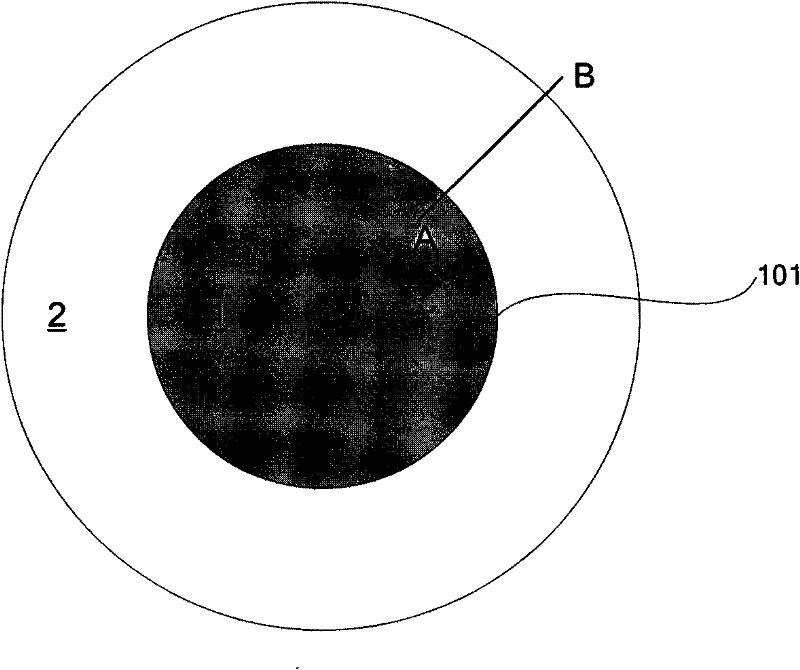
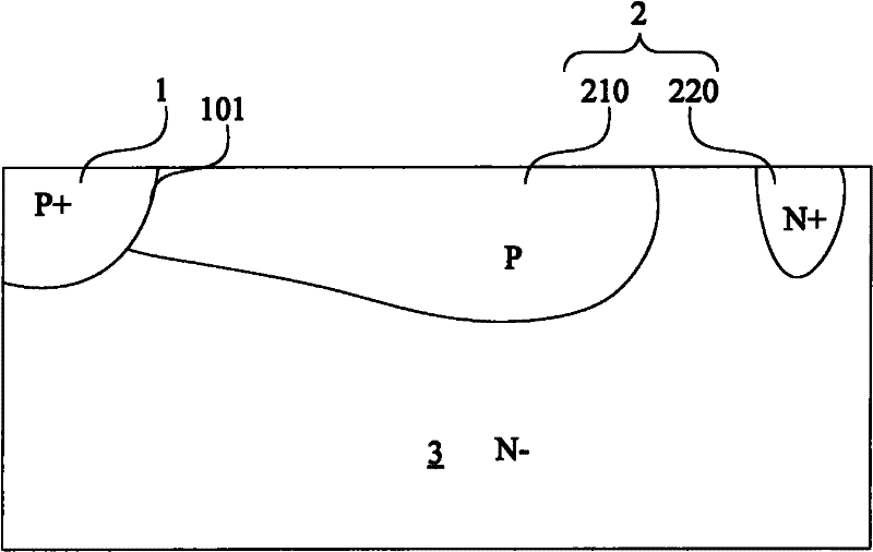
[0030] figure 2 It is a cross-sectional view of a power semiconductor with a terminal according to the first embodiment of the present invention, which is figure 1 Cut along the line AB. In this embodiment, the first conductivity type is N type, the second conductivity type is P type, and the terminal has a junction terminal extension region (JIE structure) doped with the second conductivity type (P type), and the junction termination extension region The doping thickness of the junction terminal extension region increases as the distance from the active region increases, and the doping concentration of the junction terminal extension region decreases as the distance from the active region increases. The doping thickness of the junction terminal extension region, that is, the depth of the JTE structure, is referred to as the JTE junction depth. Such as figure 2 As shown, the power semiconductor device having the terminal of the first embodiment of the present invention i...

Embodiment 2

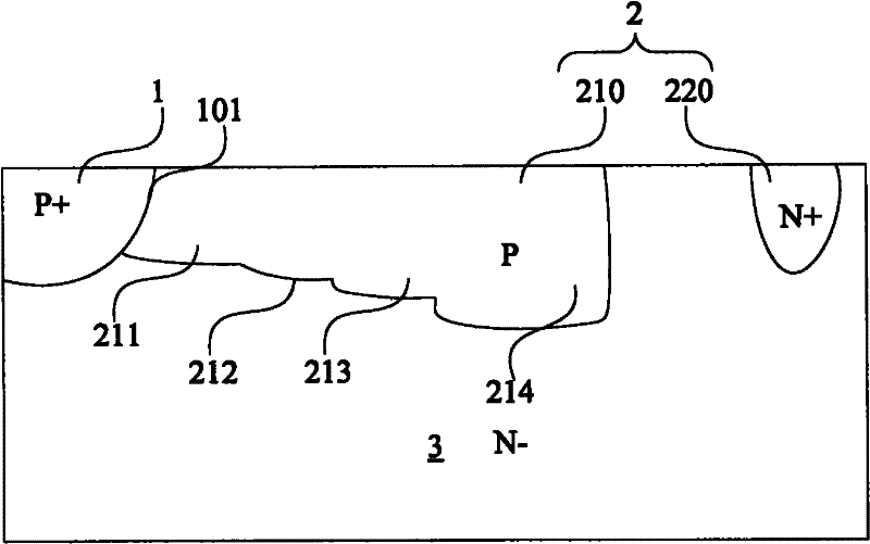
[0036] image 3 It is a cross-sectional view of a power semiconductor with a terminal according to the second embodiment of the present invention, which is figure 1 Cut along the line AB. Such as image 3 As shown, the difference between the technical solution of this embodiment and the technical solution of the first embodiment is that: the P-type JTE structure 210 is divided into several sections, and the JTE junction depths in each section are the same, but the JTE junction depths of all sections are gradually deepened, At the same time, the P-type JTE structure 210 also satisfies that the doping concentration in each section is the same, and the doping concentration in the section that is farther away from the main junction 101 is lower. The P-type JTE structure 210 in this embodiment is divided into four sections, namely the first section 211, the second section 212, the third section 213, and the fourth section 214. The JTE junction depths of all sections are increasi...


PUM


Abstract

The invention provides a terminal of a power semiconductor and a manufacturing method of the terminal. The power semiconductor comprises a first semiconductor layer of a first conduction type; the first semiconductor layer contains an active region of a well region doped with a second conduction type; the terminal is positioned in the first semiconductor layer, and comprises a junction terminal expansion region adjacent to the active region and doped with a second conduction type; the doping thickness of the junction terminal expansion region increases along with the increase of the distance to the active region; and the doping concentration of the junction terminal expansion region decreases along with the increase of the distance to the active region. In the terminal structure of the invention, the resistivity of the junction terminal expansion increases along with the decrease of the doping concentration; and the cross sectional area within unit length increases along with the increase of the doping thickness, thus relieving the resistance raising caused by the degression of the doping concentration, leading that the potential distribution of the terminal is even, effectively avoiding the premature breakdown from occurring locally, and improving the tolerable voltage of the terminal.

Description

technical field [0001] The invention relates to a terminal structure of a semiconductor device, in particular to a terminal of a power semiconductor device and a manufacturing method thereof. Background technique [0002] Due to the junction bending phenomenon, the terminals of power semiconductor devices often suffer from premature breakdown. Therefore, the design of the terminal protection structure has become an important part of the optimal design of power semiconductor devices, especially high-voltage and high-power devices. [0003] Currently, the more common termination protection structures include field rings, field plates, junction termination extensions (JTE), bevels, trenches, and so on. It is difficult to realize the oblique angle and trench structure, and the field ring and field plate consume a large area, which reduces the utilization rate of the silicon wafer and is greatly affected by the interface charge. Figure 4 It is a schematic diagram of a terminal ...

Claims


Application Information

Patent Timeline
Patent Type & Authority Patents(China)
IPC IPC(8): H01L29/06H01L29/36H01L21/02H01L21/22
Inventor 肖秀光孙超
Owner BYD SEMICON CO LTD
Why Eureka
Try Eureka