A mixed trimming method

A punching and bonding technology, which is applied in the direction of electrical components, semiconductor/solid-state device manufacturing, circuits, etc., can solve the problems of bonding interface peeling, transfer layer peeling, etc., to improve utilization, reduce heating and/or stress Effect

Inactive Publication Date: 2011-04-13
SOITEC SA
View PDF2 Cites 4 Cited by
  • Summary
  • Abstract
  • Description
  • Claims
  • Application Information

AI Technical Summary

Problems solved by technology

[0005] However, such die-cutting can cause the problem of flaking at the bonding interface between the transfer layer and the support, as well as flaking in the transfer layer itself

Method used


Image

  • A mixed trimming method
  • A mixed trimming method
  • A mixed trimming method

Examples


Embodiment Construction

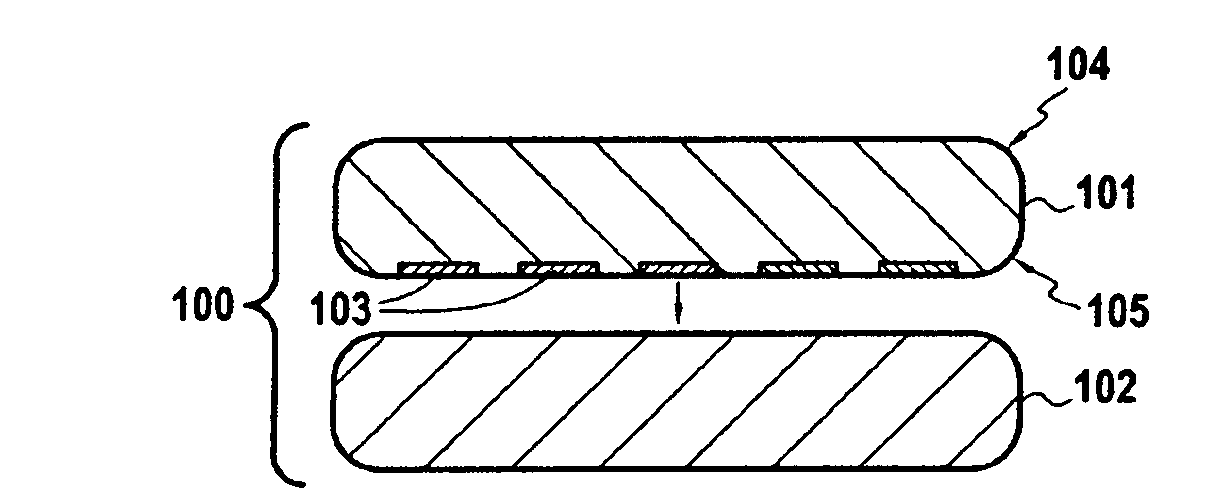
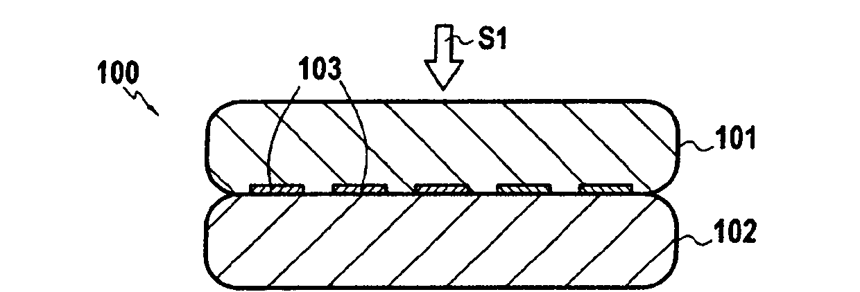
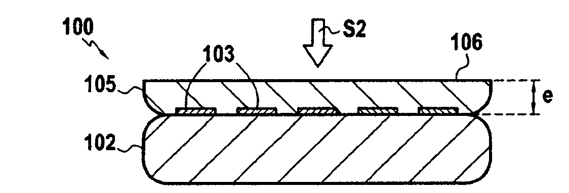
[0023] The invention generally applies to die-cutting structures comprising at least two wafers bonded together by molecular bonding or any other type of bonding (e.g., anodic, metallic, or adhesive bonding) such that The components are preformed in a first wafer which will later be bonded to a second wafer forming the support. Wafers are generally circular and can have different diameters, in particular 100 mm (millimetres), 200 mm or 300 mm in diameter. As used herein, the term "component" refers to any type of component fabricated from a material other than the wafer material and sensitive to high temperatures, typically those used to strengthen the bonding interface. These components correspond in particular to an element or a plurality of electronic microcomponents forming all or part of an electronic component, such as circuits, contacts or active layers, which components may be damaged or even destroyed if exposed to high temperatures. Components may also correspond to...


PUM


Abstract

The invention relates to a method of trimming a structure (500) comprising a first wafer (200) bonded to a second wafer (300), the first wafer (200) having a chamfered edge. The method comprises a first step (S4) for trimming the edge of the first wafer (200) carried out by mechanical machining over a predetermined depth (Pd1) in the first wafer. This first trimming step is followed by a second step (S5) for non-mechanical trimming over at least the remaining thickness of the first wafer.

Description

technical field [0001] The invention relates to the field of manufacturing multilayer semiconductor structures or substrates, also called multilayer semiconductor wafers, produced by transferring at least one layer onto a support. The transfer layer is formed by molecularly bonding a first wafer, usually thinned after bonding, to a second wafer or support. Said first wafer may also comprise all or part of a component, or a plurality of microcomponents, which, when occurring together with three-dimensional (3D) integration of components, requires the transfer of one or more layers of microcomponents to a final support, And it also occurs with circuit transfer, for example, in the manufacture of backlit imaging devices. Background technique [0002] The edges of the wafers used to form the transfer layer and support usually have chamfers or edge roundings which facilitate handling of the wafers and avoid breakage at the edges if these edges protrude. Particulates that contam...

Claims


Application Information

Patent Timeline
Patent Type & Authority Applications(China)
IPC IPC(8): H01L21/302
CPCH01L21/302H01L21/76256
Inventor M·布鲁卡特M·米热蒂S·莫利纳里E·内雷
Owner SOITEC SA
Why Eureka
Try Eureka