Semiconductor structure and forming method thereof

A semiconductor and electrode layer technology, which is applied in the fields of semiconductor/solid-state device manufacturing, electrical components, circuits, etc., and can solve the problem that the formation method of semiconductor structure needs to be improved.

Pending Publication Date: 2021-02-09
SEMICON MFG INT (SHANGHAI) CORP +1
View PDF0 Cites 1 Cited by
  • Summary
  • Abstract
  • Description
  • Claims
  • Application Information

AI Technical Summary

Problems solved by technology

[0005] However, the semiconductor structure and its formation...

Method used


Image

  • Semiconductor structure and forming method thereof
  • Semiconductor structure and forming method thereof
  • Semiconductor structure and forming method thereof

Examples


no. 1 example

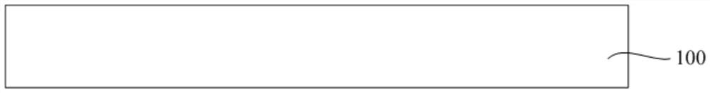
[0037] refer to figure 1 , providing a substrate 100.

[0038]In this embodiment, the material of the substrate 100 is silicon. In other embodiments, the material of the substrate is germanium.

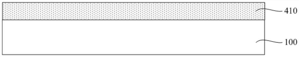
[0039] refer to figure 2 , forming a first electrode layer 410 on the substrate 100 .

[0040] In this embodiment, the material of the first electrode layer 410 is titanium nitride. In other embodiments, the material of the first electrode layer is tantalum nitride.

[0041] The first electrode layer 410 is formed by chemical vapor deposition or atomic layer deposition.

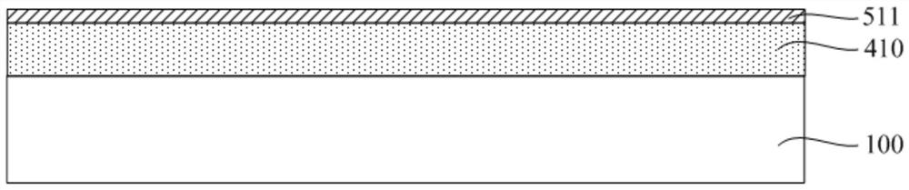
[0042] refer to image 3 , forming a dielectric layer 511 on the first electrode layer 410 .

[0043] The material of the dielectric layer 511 is a high-K dielectric material. In this embodiment, the material of the dielectric layer 511 is HfO 2 ; In other embodiments, the material of the dielectric layer can also be HfSiO, HfSiON, HfTaO, HfTiO, HfZrO or ZrO 2 .

[0044] refer to Figure 4 , forming the...

no. 2 example

[0060] refer to Figure 10 , providing a substrate 100.

[0061] In this embodiment, the material of the substrate 100 is silicon. In other embodiments, the material of the substrate is germanium.

[0062] In this embodiment, the substrate 100 includes a first region I and a second region II.

[0063] refer to Figure 11 , form a dielectric layer 200 on the surface of the substrate 100; etch the dielectric layer 200 to form a plurality of through holes in the dielectric layer 200; form a conductive layer 210 that fills the through holes, and the conductive layer 210 The top is flush with the top of the dielectric layer 200 .

[0064] The material of the dielectric layer 200 is insulating material. In this embodiment, the material of the dielectric layer 200 is silicon oxide. In other embodiments, the material of the dielectric layer is silicon nitride, silicon carbonitride, silicon oxycarbonitride, silicon oxynitride, boron nitride or boron carbonitride.

[0065] In thi...

no. 3 example

[0118] The difference between this embodiment and the second embodiment will be described in detail below. For the formation of the first electrode layer 410 and the previous process steps, reference may be made to the second embodiment, and details are not repeated here.

[0119] refer to Figure 24 and Figure 25 , forming a dielectric layer 511 on the first electrode layer 410 ; forming a second electrode layer 421 on the dielectric layer 511 .

[0120] In this embodiment, the dielectric layer 511 exposes part of the surface of the first electrode layer 410 , and the dielectric layer 511 includes a plurality of sub-dielectric structures 510 arranged in a discrete manner.

[0121] In this embodiment, the second electrode layer 421 includes a plurality of second sub-electrode structures 420 , and the second sub-electrode structures 420 correspond to the sub-dielectric structures 510 one by one.

[0122] The method for forming the dielectric layer 511 and the second electro...


PUM


Abstract

The invention discloses a semiconductor structure and a forming method thereof. The forming method comprises the steps: providing a substrate; forming a first electrode layer on the substrate; forminga dielectric layer on the first electrode layer; forming a second electrode layer on the dielectric layer; forming an oxide layer on the second electrode layer; forming a first etching stop layer onthe surface of the oxide layer; forming an insulating layer on the first etching stop layer; and etching the insulating layer, the first etching stop layer and the oxide layer to form a first contacthole, wherein the bottom of the first contact hole expose the top surface of the second electrode layer, and the first contact hole penetrates through the insulating layer, the first etching stop layer and the oxide layer. According to the invention, the adhesion strength of the second electrode plate and the first etching stop layer is improved, and the risk of layering between the second electrode plate and the first etching stop layer is reduced, so that the packaging quality is improved.

Description

technical field [0001] The invention relates to the technical field of semiconductor manufacturing, in particular to a semiconductor structure and a forming method thereof. Background technique [0002] An integrated circuit is a tiny electronic device. Specifically, an integrated circuit integrates electronic components such as transistors, diodes, resistors, capacitors, and inductors through wiring interconnections on a semiconductor wafer or a dielectric substrate. Due to the extremely small size of the integrated circuit, the integrated circuit works extremely fast and with high reliability. [0003] Integrated circuit packaging refers to dividing the processed wafer into multiple chips, and connecting the contacts on the chip to the pins of the package shell with wires, and these pins are connected to other devices through the wires on the printed board, so that It finally forms a path connected to an external power source. [0004] The quality of integrated circuit ...

Claims


Application Information

Patent Timeline
IPC IPC(8): H01L21/04H01L21/768
CPCH01L21/043H01L21/76847H01L21/76879
Inventor 胡连峰
Owner SEMICON MFG INT (SHANGHAI) CORP
Why Eureka
Try Eureka