
Method for making aluminum soldering disc

A manufacturing method and a technology of aluminum pads, which are applied in semiconductor/solid-state device manufacturing, electrical components, circuits, etc., can solve problems such as uneven distribution, affecting the physical appearance of aluminum pads, bonding wires, and uneven thicknesses

Inactive Publication Date: 2011-04-20
SEMICON MFG INT (SHANGHAI) CORP
View PDF2 Cites 10 Cited by
  • Summary
  • Abstract
  • Description
  • Claims
  • Application Information

AI Technical Summary

Problems solved by technology

[0003] However, in practical applications, after the PVD process is used to form the aluminum film layer, since metal aluminum is easily oxidized in the air, it will form 20 angstroms to 35 angstroms on the surface of the aluminum pad with different thickness and uneven distribution. , dense alumina (Al 2 o 3 ) film, when the aluminum pad is wet-cleaned with a cleaning agent containing HF, the water contained in HF and HF will interact with Al 2 o 3 The chemical reaction of the thin film produces aluminum fluoride (AlF 3 ) and aluminum hydroxide (Al(OH) 3 ), and the air humidity of the factory is generally greater than 50%, the water vapor in the air and Al 2 o 3 The chemical reaction of the film will also generate Al(OH) 3 , AlF 3 and Al(OH) 3 Both will cause crystal-like defects on the surface of the aluminum pad, which will affect the physical appearance of the aluminum pad and subsequent bonding connections

Method used


Image

  • Method for making aluminum soldering disc
  • Method for making aluminum soldering disc

Examples


Embodiment Construction

[0016] In order to make the object, technical solution and advantages of the present invention clearer, the present invention will be further described in detail below with reference to the accompanying drawings and examples.

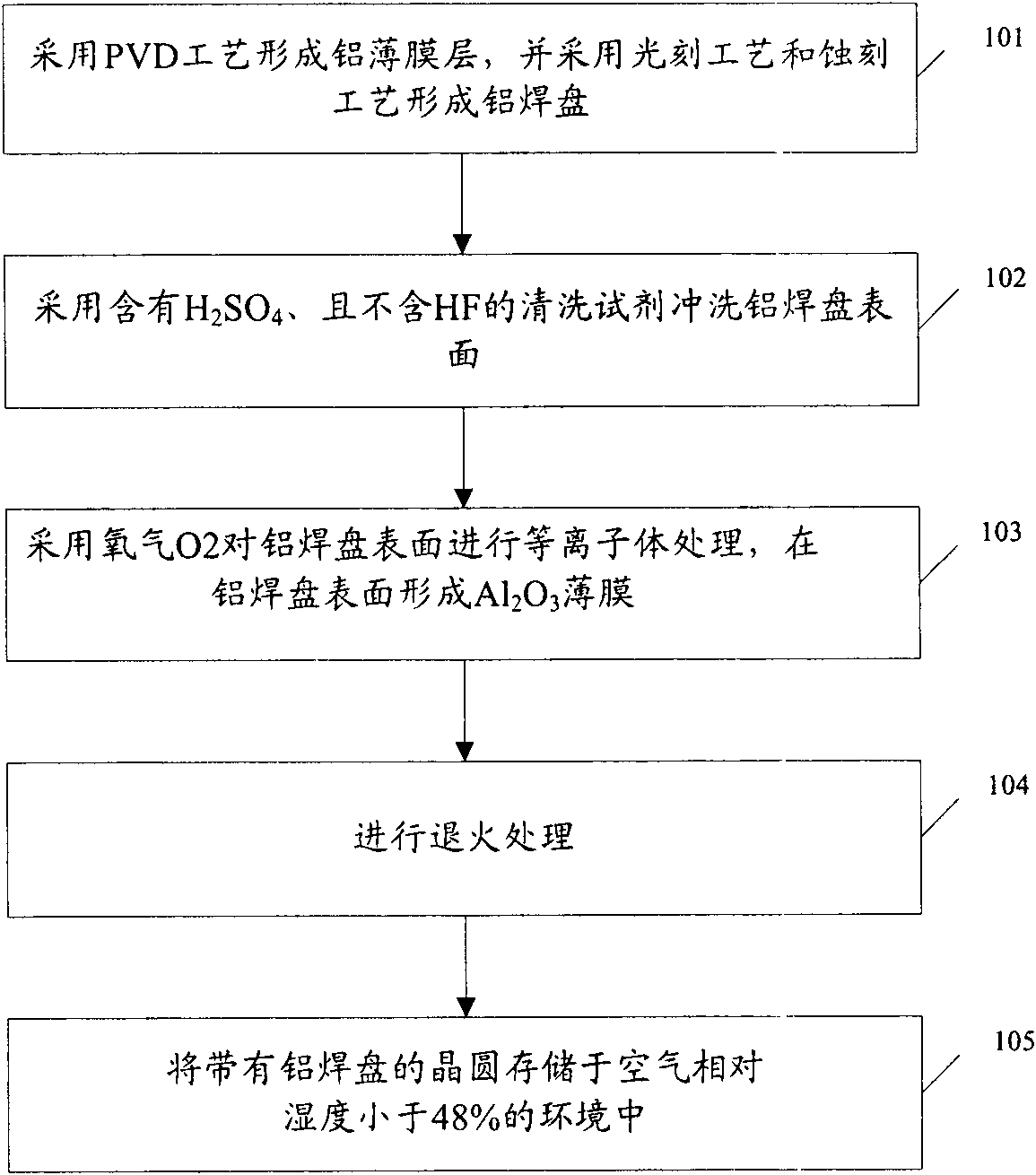
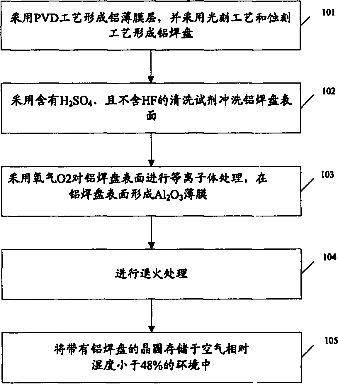
[0017] figure 1 The flow chart of the manufacturing method of the aluminum pad provided by the present invention, such as figure 1 As shown, the method includes the following steps:

[0018] In step 101, an aluminum film layer is formed on the surface of the wafer by PVD technology, and an aluminum pad is formed by photolithography technology and etching technology.

[0019] The content of this step is the prior art, and will not be repeated here.

[0020] Step 102, adopt containing sulfuric acid (H 2 SO 4 ) and HF-free cleaning reagent to rinse the surface of the aluminum pad.

[0021] In this step, the H 2 SO 4 The cleaning reagent of the prior art replaces the cleaning reagent containing HF in the prior art, thereby avoiding AlF 3 generation,...


PUM

PropertyMeasurementUnit
Thicknessaaaaaaaaaa

Abstract

The invention provides a method for making an aluminum soldering disc. The method comprises the following steps of: forming an aluminum film layer on the surface of a wafer by using a PVD (Physical Vapor Deposition) process; forming an aluminum disc by using a photoetching process and an etching process; and then flushing the surface of the aluminum disc with a cleaning reagent containing sulfuric acid (H2SO4); carrying out plasma treatment on the surface of the aluminum disc with oxygen (O2) to form an aluminum oxide (Al2O3) film on the surface of the aluminum disc; and performing annealing treatment. By using the method, a crystal shaped defect on the surface of the aluminum soldering disc can be avoided.

Description

technical field [0001] The invention relates to the field of semiconductor manufacturing, in particular to a method for manufacturing an aluminum pad. Background technique [0002] With the wide application of electronic equipment, the manufacturing process of semiconductors has been developed rapidly. In the manufacturing process of semiconductors, it involves the production method of aluminum pads. The aluminum pads are the interconnection interface between the wafer and the outside world. Bonding wires on the surface of the aluminum pads allow the wafer to form a metallic connection to the outside world. In the prior art, the manufacturing method of the aluminum pad includes: adopting physical vapor deposition (PVD) process to form an aluminum film layer on the entire wafer surface, adopting a photolithography process and an etching process to form an aluminum pad, and then aluminum pad Wet cleaning, final annealing, and the wafers with aluminum pads are stored in the fa...

Claims


Application Information

Patent Timeline
IPC IPC(8): H01L21/60H01L21/321
Inventor 徐长春王艳琴王晓艳陈其道
Owner SEMICON MFG INT (SHANGHAI) CORP
Learn More