Growth method for growing silicon carbide crystals by PVT method

A growth method and technology of silicon carbide, applied in chemical instruments and methods, single crystal growth, crystal growth and other directions, can solve the problems of low quality of silicon carbide crystal growth, crystal defects, etc., to reduce carbon inclusion defects, improve quality, The effect of avoiding crystal defects

Active Publication Date: 2020-12-29
中电化合物半导体有限公司
View PDF6 Cites 3 Cited by
  • Summary
  • Abstract
  • Description
  • Claims
  • Application Information

AI Technical Summary

Problems solved by technology

[0014] In view of the above-mentioned shortcomings of the prior art, the object of the present invention is to provide a growth method for growing silicon carbide crystals by PVT method, which is used to solve the problem of silicon-rich vapor deposition on the crystal when the PVT method is used to form silicon carbide crystals in the prior art. The surface condenses into silicon droplets to form crystallization defects, resulting in problems such as lower quality of silicon carbide crystal growth

Method used


Image

  • Growth method for growing silicon carbide crystals by PVT method
  • Growth method for growing silicon carbide crystals by PVT method
  • Growth method for growing silicon carbide crystals by PVT method

Examples


Embodiment 1

[0056] As mentioned in the background technology, in the initial stage of silicon carbide crystal growth, the growth atmosphere is rich in gaseous silicon, and under the action of axial temperature gradient, the steam is transported to the low-temperature silicon carbide seed crystal region, and the saturated vapor pressure of the silicon-rich gas phase decreases, condensing into Liquid-phase silicon causes crystallization defects. In order to overcome this defect, gas that can react with silicon vapor at high temperature is usually introduced into the silicon carbide raw material to form silicide, thereby removing gas-phase silicon in the growth atmosphere. However, silicon carbide crystals produced by this method still have crystal defects.

[0057] Based on the above-mentioned problems and detailed analysis of various factors, the inventor determined that the main reason for the crystallization defects in silicon carbide crystals is that the uniformity of chlorine-containing...

Embodiment 2

[0071] This embodiment provides a method for growing silicon carbide crystals, which is realized based on the crucible for growing silicon carbide crystals by the PVT method described in Embodiment 1. For the beneficial effects that the crucible can achieve, please refer to Embodiment 1, as follows No longer.

[0072] Such as Figure 2 to Figure 4 As shown, the growth method comprises the steps of:

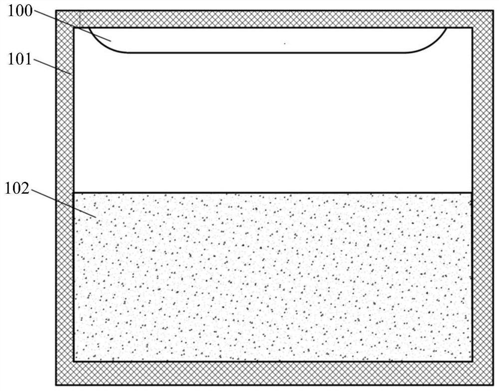
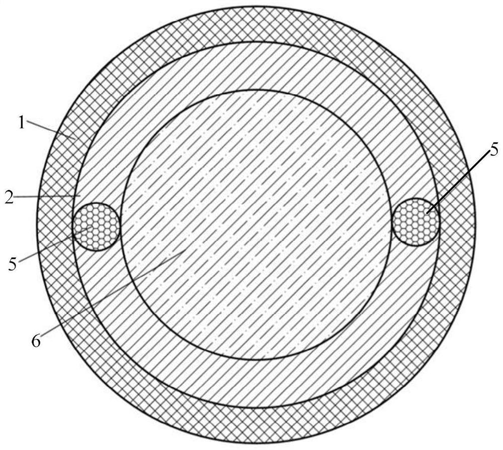
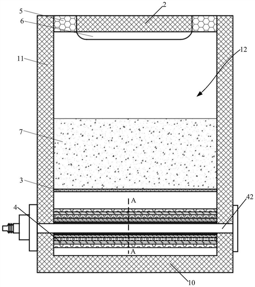
[0073] 1) Provide a crucible for growing silicon carbide crystals by PVT method as described in Embodiment 1, and place a silicon carbide raw material 7 on a porous graphite plate 3 in the crucible and place a silicon carbide seed above the accommodating chamber 12 of the crucible Crystal 6;

[0074] 2) Put the crucible into the silicon carbide single crystal growth chamber. The silicon carbide single crystal growth chamber is mainly used for heating. Generally, the silicon carbide single crystal growth temperature is above 2000°C, and eddy current heating is adopted, that is, ...


PUM

PropertyMeasurementUnit
Outer diameteraaaaaaaaaa
Thicknessaaaaaaaaaa
Outer diameteraaaaaaaaaa

Abstract

The invention provides a growth method for growing silicon carbide crystals by a PVT method. The method comprises the following steps: providing a crucible; placing a silicon carbide raw material anda seed crystal in the crucible; putting the crucible into a growth chamber, vacuumizing, introducing protective gas, and setting the temperature of the chamber; raising the temperature to a first preset temperature, introducing chlorine-containing gas through a gas dispersing device in the crucible, raising the temperature to a second preset temperature, and stopping introducing the chlorine-containing gas or continuously introducing the chlorine-containing gas for a first preset time; raising the temperature to a third preset temperature, and annealing to obtain the silicon carbide crystal after the silicon carbide crystal starts to grow for a second preset time. According to the growth method, the release rate and uniformity of the chlorine-containing gas can be effectively controlled, and the crystallization defect caused by condensation of gas-phase silicon on the surface of the crystal is avoided; by controlling the introduction time and flow of the chlorine-containing gas, the crystallization defect can be further avoided; due to the arrangement of the porous graphite block, introduced excessive chlorine-containing gas and carbon particles suspended in a growth atmosphere canbe dissipated, and the defects of carbon inclusions in crystals are reduced.

Description

technical field [0001] The invention relates to the technical field of silicon carbide crystal preparation, in particular to a method for growing silicon carbide crystals by a PVT method. Background technique [0002] Compared with silicon-based semiconductors, the third-generation semiconductors represented by silicon carbide have the characteristics of forbidden bandwidth, high saturated electron mobility, high breakdown electric field strength, and high thermal conductivity. They have high frequency, high temperature resistance, chemical corrosion resistance, High efficiency, strong radiation resistance, high pressure resistance and other superior performance, with the increasingly mature silicon carbide semiconductor preparation technology, will increasingly become an Supporting materials for core electronic devices in fields such as petroleum exploration and production. [0003] Silicon carbide crystal preparation methods include high temperature chemical vapor deposit...

Claims


Application Information

Patent Timeline
IPC IPC(8): C30B23/00C30B29/36
CPCC30B23/002C30B29/36
Inventor 陈豆薛卫明马远
Owner 中电化合物半导体有限公司
Why Eureka
Try Eureka