Focusing and levelling device with expandable measuring range and focusing and levelling method

A technology of focusing and leveling device and measuring range, which is applied to the exposure device of photo-engraving process, photo-engraving process of pattern surface, optics, etc. The effect of measuring intervals

Active Publication Date: 2011-04-27
SHANGHAI MICRO ELECTRONICS EQUIP (GRP) CO LTD
View PDF1 Cites 30 Cited by
  • Summary
  • Abstract
  • Description
  • Claims
  • Application Information

AI Technical Summary

Problems solved by technology

[0004] This technology can achieve high measurement accuracy, but its measurement principle determines that its measurement range is greatly affected by the amplitude of the scanning mirror and the size of the measurement spot in the scanning direction.
To obtain a larger measurement range, a scanning mirror with a larger amplitude is required, which puts forward higher requirements on the performance of the scanning mirror, and makes the mechanical structure of the measurement system more bulky

Method used


Image

  • Focusing and levelling device with expandable measuring range and focusing and levelling method
  • Focusing and levelling device with expandable measuring range and focusing and levelling method
  • Focusing and levelling device with expandable measuring range and focusing and levelling method

Examples


no. 1 example

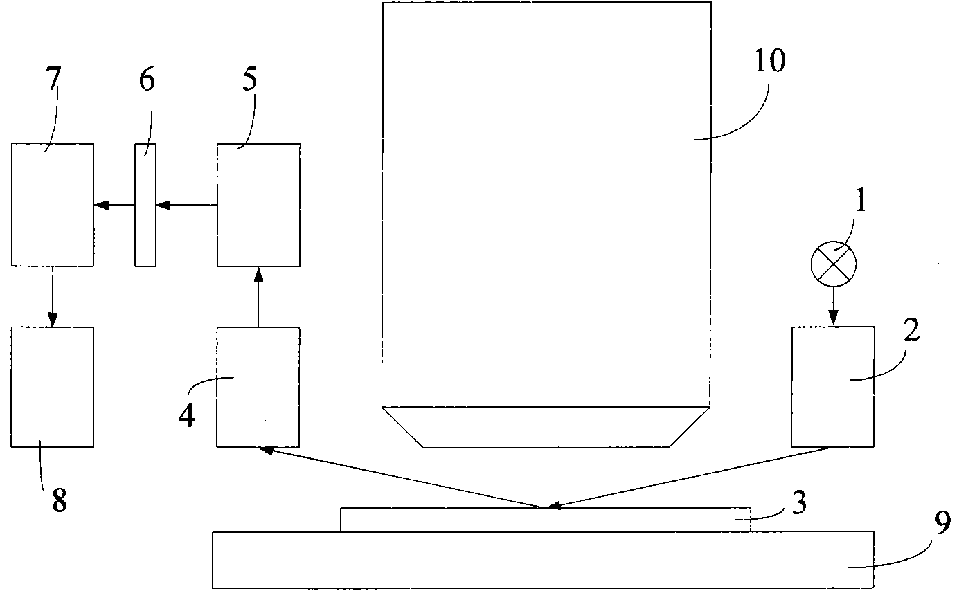
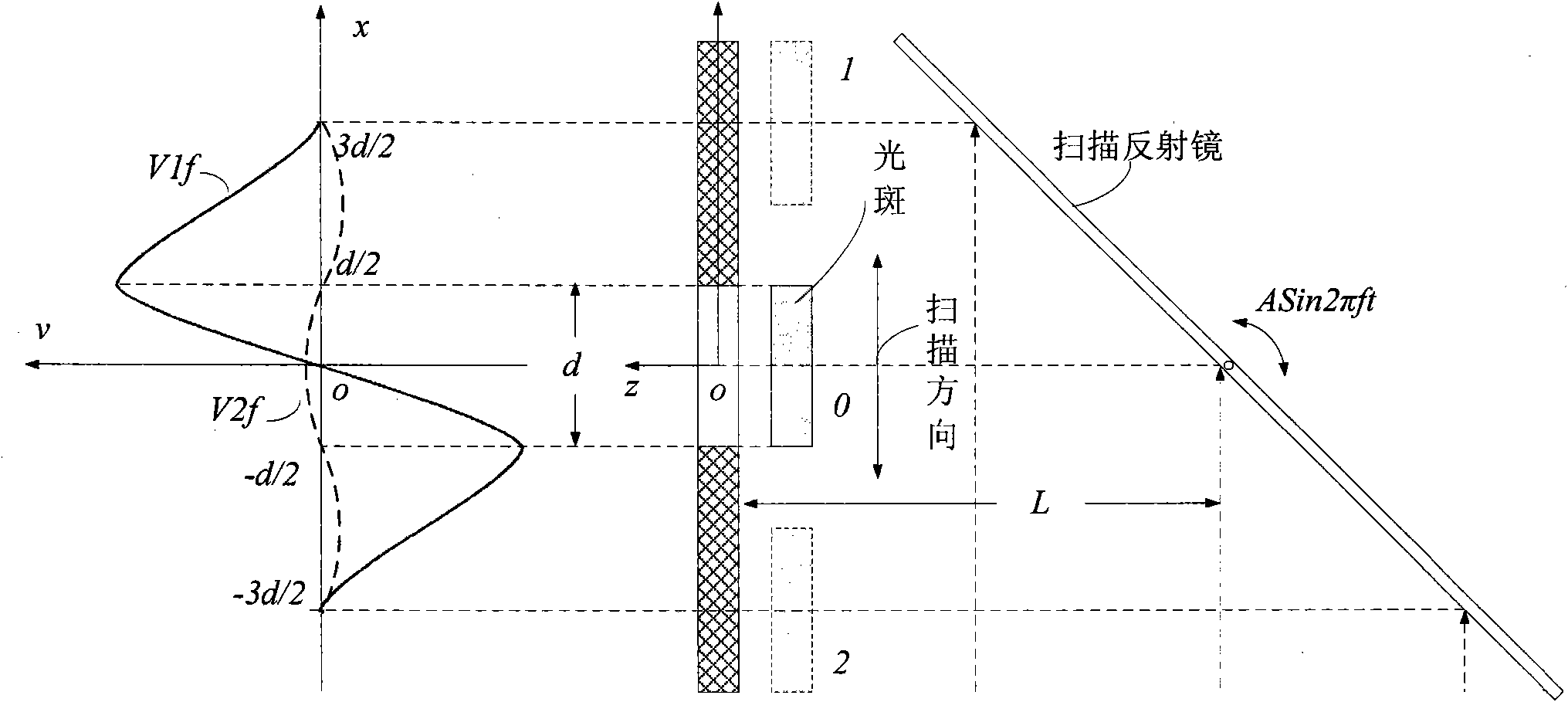
[0054] figure 1Shown is a structural diagram of a focusing and leveling measurement device used in projection lithography equipment according to the present invention. Wherein the measured silicon wafer 3 is located directly below the projection objective lens 10 and is supported by the workpiece table 9 . The light source 1, the optical projection unit 2, the tested silicon wafer 3, the optical receiving unit 4, the optical modulation unit 5, the receiving slit surface 6, the photodetector 7 and the control unit 8 constitute a focusing and leveling device. The device is used to realize the measurement of the surface height and inclination information of the silicon wafer 3 . The probe light emitted by the light source 1 irradiates the surface of the silicon wafer 3 through the optical projection unit 2 to form a measurement spot, and is reflected from the surface of the silicon wafer 3, passes through the optical receiving unit 4 and the optical modulation unit 5, and is fin...

no. 2 example

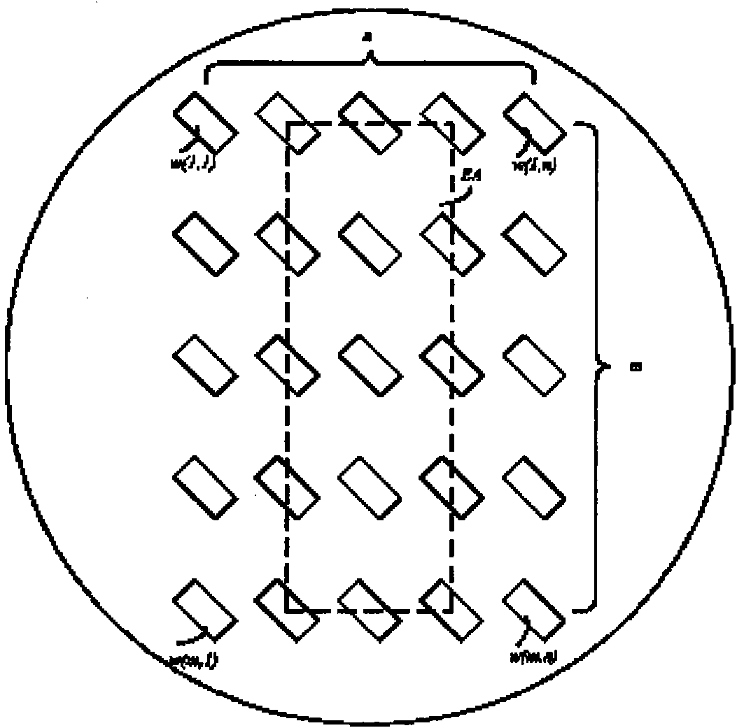
[0060] In the first embodiment, only the measurement range of two points (s(m, 1) and s(1, n)) is extended, and only the height value of the measured surface can be given within the extended range, and the inclination cannot be adjusted , so there are certain requirements for the inclination range of the silicon wafer. If the inclination of the silicon wafer is relatively large, it is difficult to level the silicon wafer using the process of Embodiment 1, and a pre-step is required to level the silicon wafer to a certain extent. In order to obtain inclination information within the extended measurement range, a group of extended slits can be added on the receiving slit plane. Figure 8 Shown is a distribution diagram of the slit matrix on the receiving slit plane in the focusing and leveling device according to the second embodiment of the present invention. By adding slits sx5 and slits sx6 on both sides of the slit s(m, 3) in the area C, the height values ​​of three points c...


PUM


Abstract

The invention relates to a focusing and levelling device with an expandable measuring range, which comprises a light source, an optical projection unit, an optical receiving unit, an optical modulation unit, a receiving silt surface, a photoelectric detector and a control unit, wherein the optical projection unit receives light emitted by the light source and irradiates the light to the surface of a measured silicon wafer to form a measuring light spot matrix W; the optical receiving unit receives the light reflected by the measured silicon wafer; the optical modulation unit is provided with a scanning reflector which makes sinusoidal vibration during levelling measurement; a silt matrix S of silts corresponding to each light spot on the silicon wafer is formed on the receiving silt surface, and the light spots reflected by the scanning reflector are imaged on the receiving silt surface; the photoelectric detector converts a light energy signal passing through the silts into an electrical signal; the control unit analyzes the electrical signal outputted by the photoelectric detector; and an expanding silt positioned on the edge of the silt matrix is also formed on the receiving silt surface and is used for expanding the measuring range of the focusing and levelling device. The invention also discloses a focusing and levelling method using the device.

Description

technical field [0001] The invention relates to photolithographic equipment in the field of integrated circuit or other micro-device manufacturing, and in particular to a focusing and leveling device and method for performing focusing and leveling measurements on silicon wafers. Background technique [0002] In projection lithography equipment, a focusing and leveling measuring device is usually used to measure the height and inclination of a specific area on the surface of a silicon wafer. In the current scanning projection lithography apparatus, the optical measurement method is mostly used to realize the focus and leveling measurement of the silicon wafer. [0003] U.S. Patent U.S.4,558,949 (Horizontal position detecting device, applied on September 17, 1982) discloses a focusing and leveling measurement device. The device has two independent measurement systems, which are respectively used for the height and inclination of a specific area of ​​the silicon wafer. degree ...

Claims


Application Information

Patent Timeline
Patent Type & Authority Applications(China)
IPC IPC(8): G03F9/00G03F7/20
Inventor 潘炼东李志丹陈飞彪张冲
Owner SHANGHAI MICRO ELECTRONICS EQUIP (GRP) CO LTD
Why Eureka
Try Eureka