Supercharge Your Innovation With Domain-Expert AI Agents!

Method and system for processing graphs

A processing method and graphic technology, applied in chemical/electrolytic methods to remove conductive materials, printed circuits, electrical components, etc., can solve the problems of complex implementation, high process requirements, poor dry film analysis, etc., and achieve high accuracy. Effect

Inactive Publication Date: 2011-05-11
PEKING UNIV FOUNDER GRP CO LTD +1
View PDF2 Cites 8 Cited by
  • Summary
  • Abstract
  • Description
  • Claims
  • Application Information

AI Technical Summary

Problems solved by technology

This situation is called poor dry film analysis, which is not conducive to the processing of graphics in subsequent processes.
[0004] In addition, the required pattern is transferred to the dry film by means of film exposure, and the thickness of the dry film must be very small, otherwise the exposure effect will be seriously affected.
It is generally required that the thickness of the dry film is not greater than 30 microns, which requires a higher process and is more complicated to realize.

Method used


Image

  • Method and system for processing graphs
  • Method and system for processing graphs
  • Method and system for processing graphs

Examples


Embodiment Construction

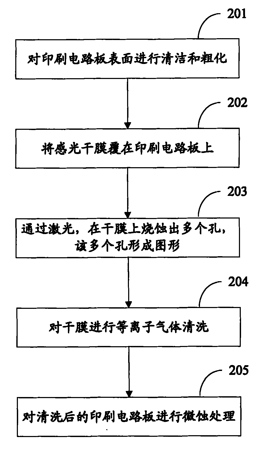
[0028] In the embodiment of the present invention, a plurality of holes are ablated on the dry film by means of laser drilling, and the plurality of holes form a pattern, which realizes pattern processing and solves the problems caused by exposure and development. Moreover, in the embodiment of the present invention, only the dry film is ablated during hole burning, and the printed circuit board under the photosensitive dry film is not ablated.

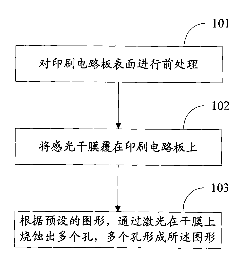
[0029] see figure 1 , the main process flow of graphics processing in this embodiment is as follows:

[0030] Step 101: Perform pretreatment on the surface of the printed circuit board. Specifically, the surface of the printed circuit board is cleaned and roughened.

[0031] Step 102: Covering the dry film on the printed circuit board. The dry film in this embodiment can be a photosensitive dry film.

[0032] Step 103: According to the preset pattern, ablate a plurality of holes on the dry film by laser, so that the plurality of h...


PUM

PropertyMeasurementUnit
Thicknessaaaaaaaaaa

Abstract

The invention discloses a method and system for processing graphs to improve the accuracy of the graphs. The method comprises the following steps of: carrying out pre-processing on the surface of a printed circuit board; covering a sensitizing dry film on the printed circuit board; and ablating a plurality of holes on the dry film by laser according to the preset graph and making the plurality of holes form the graph. The invention further discloses a system for implementing the method.

Description

technical field [0001] The invention relates to the field of printed circuit boards, in particular to a pattern processing method and system. Background technique [0002] Since the emergence of printed circuits, the research and development of raw materials has never stopped scientific research. With the rapid development of microelectronics technology and the wide application of large-scale integrated circuits and ultra-large-scale integrated circuits, the manufacturing technology of printed circuit boards must adapt to the transfer of high-density, high-precision, thin wires, narrow spacing and small aperture circuit patterns. need. For decades, research and development of new photoresist and circuit graphics transfer technology: such as photoresist dry film, wet film technology, electrophoretic photoresist film and direct imaging technology. They are gradually adopted by manufacturers of printed circuit boards, which greatly improves the transfer quality of circuit gra...

Claims


Application Information

Patent Timeline
IPC IPC(8): H05K3/00H05K3/06
Inventor 张君容陈文德
Owner PEKING UNIV FOUNDER GRP CO LTD
Features
  • R&D
  • Intellectual Property
  • Life Sciences
  • Materials
  • Tech Scout
  • Unparalleled Data Quality
  • Higher Quality Content
  • 60% Fewer Hallucinations
Learn More