Method for processing substrate of mother board

A processing method and substrate technology, applied in stone processing equipment, stone processing tools, manufacturing tools, etc., can solve problems such as difficult marking grooves

Inactive Publication Date: 2011-05-11
MITSUBOSHI DIAMOND IND CO LTD
View PDF3 Cites 11 Cited by
  • Summary
  • Abstract
  • Description
  • Claims
  • Application Information

AI Technical Summary

Problems solved by technology

[0046] In this way, it was found that in the upper and lower substrate processing systems, it is difficult to form the desired scr

Method used


Image

  • Method for processing substrate of mother board
  • Method for processing substrate of mother board
  • Method for processing substrate of mother board

Examples


Embodiment Construction

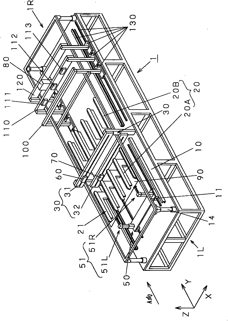
[0088] Embodiments of the substrate processing method of the present invention will be described with reference to the drawings. The substrate processing method described below is a method used in the manufacturing process of a liquid crystal display panel, specifically, a method used in a substrate processing system for dividing a unit display panel as a liquid crystal display panel from a mother board and remove them one by one.

[0089] (substrate processing system)

[0090] First, the overall configuration of a substrate processing system used for carrying out the substrate processing method of the present invention will be described.

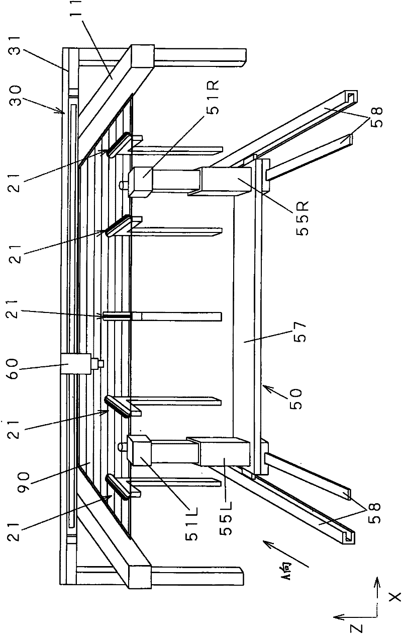
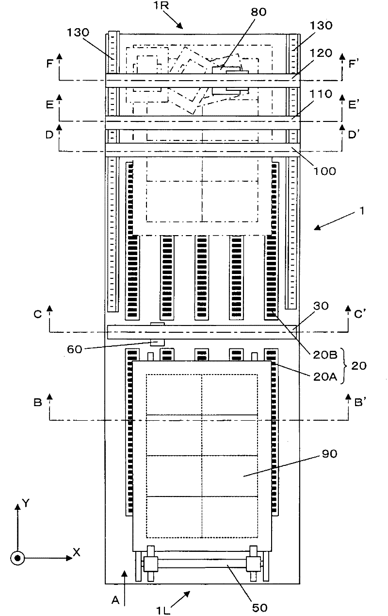
[0091] figure 1 It is a perspective view showing the overall structure of the substrate processing system 1 using the substrate processing method of the present invention. figure 2 Yes figure 1 Shown to the perspective view of A (except for the stand 10 described later). image 3 It is a top view of the substrate processing system 1 (...


PUM


Abstract

Provided is a method for processing a substrate wherein occurrence of a defective article due to adhesion of an end material region to the side of terminal cut surface is eliminated. In a method for processing the substrate of a mother board, a mother board is scribed from the opposite sides of first and second substrates by means of a cutter wheel and divided for each unit display panel, and terminal processing for exposing the terminal region of each unit display panel is performed. When scribing of a terminal region (T) between a just cut surface (Ca) and a terminal cut surface (Cb) of a mother board is performed, (a) at first, a first cutter wheel is brought into pressure contact with a position on the terminal cut surface of a first substrate (G1) and a second cutter wheel is broughtinto pressure contact with a position on the just cut surface of a second substrate (G2) in order to perform scribing simultaneously on the opposite sides, (b) and then, the first cutter wheel is brought into pressure contact with the just cut surface of a first substrate (G1) and a backup roller having no edge is brought into pressure contact with the vicinity of just cut surface of a second substrate in order to perform scribing on one side.

Description

technical field [0001] The present invention relates to a substrate processing method for a mother board, which is used to divide a mother board formed by bonding two brittle material substrates such as glass (also referred to as a bonded substrate or a bonded mother board) to form multiple substrates as processed products. A unit substrate, more specifically, relates to a substrate processing method for forming a terminal region for external connection on the periphery of the unit substrate when forming the unit substrate from a motherboard. [0002] Specifically, the substrate processing method of the present invention is used when processing unit display panels of liquid crystal display panels and the like. Background technique [0003] Two large-area glass substrates are used in the liquid crystal display panel, a color filter (color filter) is formed on one substrate, and a thin film transistor (TFT: Thin film Transistor) for driving the liquid crystal is formed on the ...

Claims


Application Information

Patent Timeline
IPC IPC(8): G02F1/13B28D1/24C03B33/07G02F1/1333G09F9/00
CPCB28D1/226B65G2249/04C03B33/03C03B33/033C03B33/07G02F1/1303G02F1/133351
Inventor 前川和哉高松生芳
Owner MITSUBOSHI DIAMOND IND CO LTD
Why Eureka
Try Eureka