Air-dielectric for subtractive etch line and via metallization

a technology of air-dielectric and dielectric line, which is applied in the direction of semiconductor devices, semiconductor/solid-state device details, electrical apparatus, etc., can solve the problems of increasing the limit of copper electroplating to fill features formed in dielectric, increasing the aspect ratio, and affecting the formation of semiconductor interconnect structures. , to achieve the effect of reliable formation of semiconductor interconnect structures

Active Publication Date: 2014-05-27
GLOBALFOUNDRIES U S INC
View PDF11 Cites 7 Cited by
  • Summary
  • Abstract
  • Description
  • Claims
  • Application Information

AI Technical Summary

Benefits of technology

[0008]According to the present invention, the problem of interconnecting multiple layers of metallization, such layers having effective air gaps positioned in regions most susceptible to capacitive coupling, is solved by forming lines as well as vias that extend above such lines within a given layer of conductive material before depositing material to form air gaps between pairs of closely spaced features within that layer. The invention enables reliable formation of semiconductor interconnect structures without multiple additional lithography steps or sacrificial dielectric material.

Problems solved by technology

As feature size continues to decrease, the limitations of copper electroplating to fill features formed in dielectric are increasingly apparent.
Shrinking the feature size generally requires higher aspect ratios, which are increasingly difficult to fill, and furthermore, the barrier layer cannot scale and hence constitutes a greater fraction of any particular feature.
Feature density can also be increased by reducing the spacing between features, but closely spaced features can suffer from increased capacitive coupling.
Low k dielectrics, having k value of 3.0 or less, can be employed but are susceptible to TDDB (time dependent dielectric breakdown) and are challenging to etch, leading to issues such as poor profile control, voids, and collapse.
Air gaps have much lower k value approaching 1.0, but pose various fabrication challenges.
However, a problem with the technique of Kim et al. can arise upon attempting to connect a subsequent layer of metal interconnections.
As feature sizes shrink, alignment of the mask with underlying wires is increasingly difficult, therefore landing (i.e., forming the vertical interconnect exactly on the underlying wire) is also.
During subsequent deposition of a next metal layer, the open air gap will fill with metal, potentially shorting the adjacent features.

Method used


Image

  • Air-dielectric for subtractive etch line and via metallization
  • Air-dielectric for subtractive etch line and via metallization
  • Air-dielectric for subtractive etch line and via metallization

Examples


Embodiment Construction

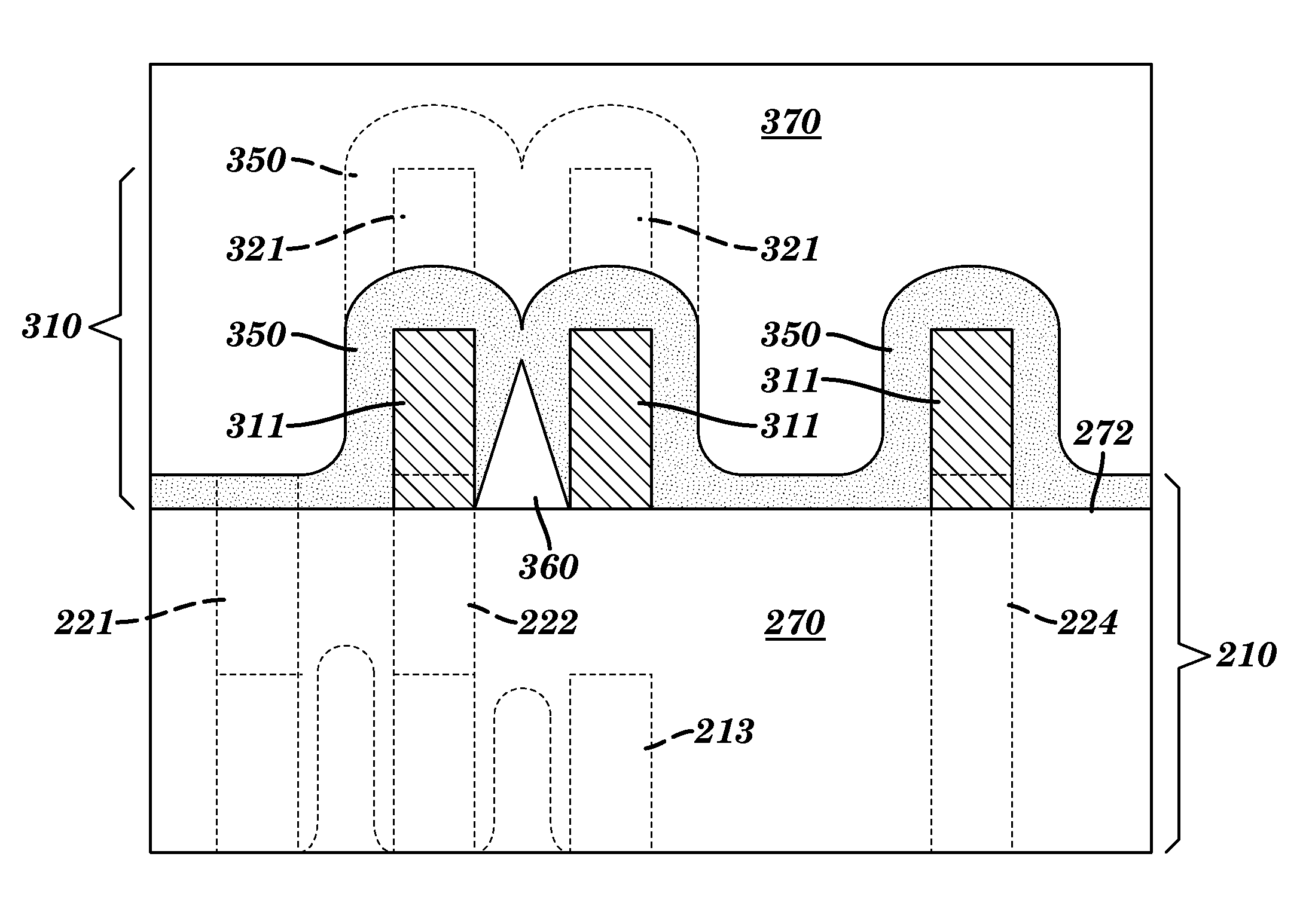
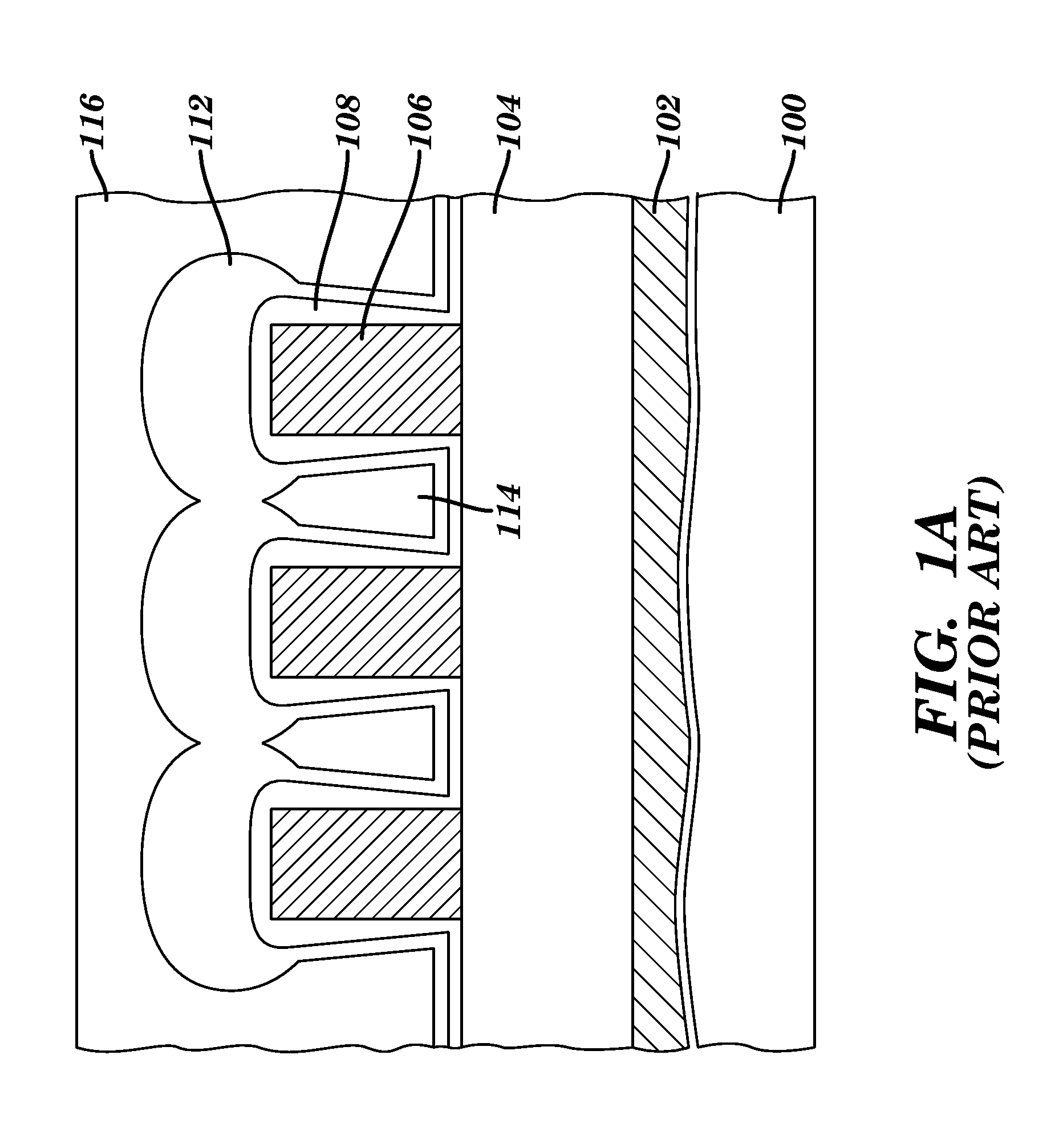
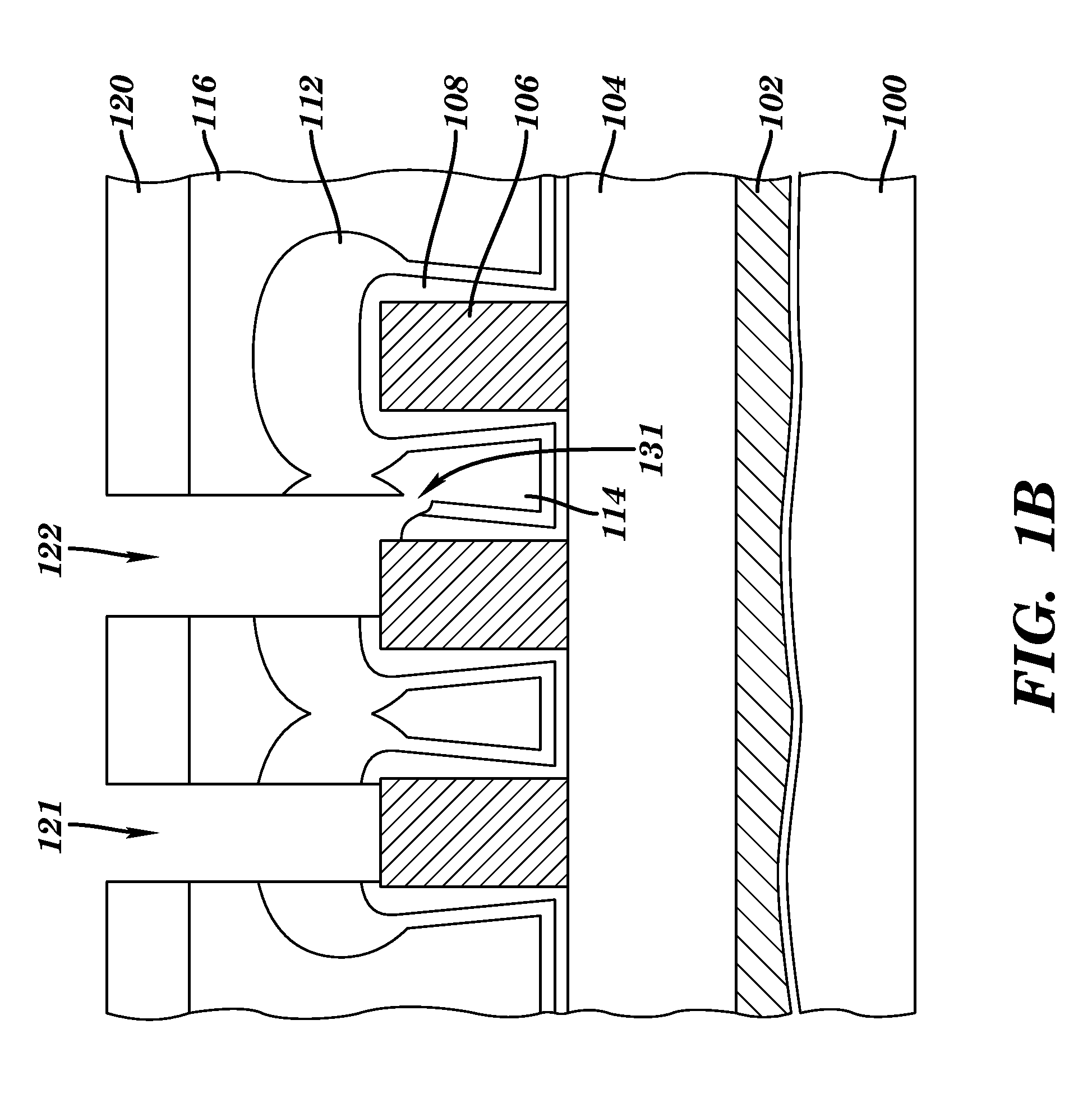
[0019]Embodiments of the present invention will now be described in greater detail by reference to the drawings that accompany the present application. It is noted that the drawings of the present application are provided for illustrative purposes only and are not drawn to scale.

[0020]In the following description, numerous specific details are set forth, such as particular structures, components, materials, dimensions, processing steps and techniques, in order to provide a thorough understanding of the present invention. However, it will be appreciated by one of ordinary skill in the art that the invention may be practiced without these specific details. In other instances, well-known structures or processing steps have not been described in detail in order to avoid obscuring the invention.

[0021]It will be understood that when an element as a layer, region or substrate is referred to as being “on” or “over” another element, it can be directly on the other element or intervening elem...


PUM


Abstract

A method and structure is disclosed whereby multiple interconnect layers having effective air gaps positioned in regions most susceptible to capacitive coupling can be formed. The method includes providing a layer of conductive features, the layer including at least two line members disposed on a substrate and spaced from one another by less than or equal to an effective distance, and at least one such line member also having a via member extending away from the substrate, depositing a poorly conformal dielectric coating to form an air gap between such line members, and exposing a top end of the via.

Description

FIELD OF THE INVENTION[0001]The present invention relates to a semiconductor structure, and a method of fabricating the same. More particularly, it relates to nano-scale semiconductor structures selectively isolated by air gaps that can be reliably formed into interconnect metallization with reduced capacitive coupling.BACKGROUND OF THE INVENTION[0002]Generally, integrated circuits include a complex network of conductive interconnects fabricated on a semiconductor substrate in which semiconductor devices have been formed. Efficient routing of these interconnects requires formation of multilevel or multilayered schemes, such as, for example, single or dual damascene wiring structures.[0003]Within an interconnect structure, conductive vias run perpendicular to the semiconductor substrate and conductive lines run parallel to the semiconductor substrate. According to conventional damascene processing, lines and vias are created within a dielectric layer. A dielectric layer is patterned ...

Claims


Application Information

Patent Timeline
Patent Type & Authority Patents(United States)
IPC IPC(8): H01L21/4763
CPCH01L23/5222H01L23/522H01L21/76802H01L23/53295H01L21/7682H01L2924/0002H01L21/76897H01L21/76885H01L2924/00
Inventor HORAK, DAVID VHUANG, ELBERTKOBURGER, CHARLES WPONOTH, SHOMYANG, CHIH-CHAO
Owner GLOBALFOUNDRIES U S INC
Why Eureka
Try Eureka