Liquid crystal display panel and liquid crystal display device

A liquid crystal display panel and liquid crystal display device technology, applied in the direction of instruments, nonlinear optics, optics, etc., can solve problems affecting product yield, increase manufacturing cost, increase manufacturing process steps, etc., achieve good liquid crystal pre-tilt effect, improve Viewing angle, effect of reducing manufacturing process steps

Active Publication Date: 2011-05-25
SHANGHAI TIANMA MICRO ELECTRONICS CO LTD
View PDF5 Cites 23 Cited by
  • Summary
  • Abstract
  • Description
  • Claims
  • Application Information

AI Technical Summary

Problems solved by technology

[0005] However, in order to realize the pre-tilt of the liquid crystal molecules in the above-mentioned liquid crystal display panel, it is necessary to add protrusions or cracks on the ITO substrate, and the protrusions and cracks need to be formed on the array substrate of the liquid crystal display panel through precise processes such as photolithography. Realization; this not only increases the manufacturing process steps, but also affects the product yield and increases the manufacturing cost

Method used


Image

  • Liquid crystal display panel and liquid crystal display device
  • Liquid crystal display panel and liquid crystal display device
  • Liquid crystal display panel and liquid crystal display device

Examples


Embodiment 1

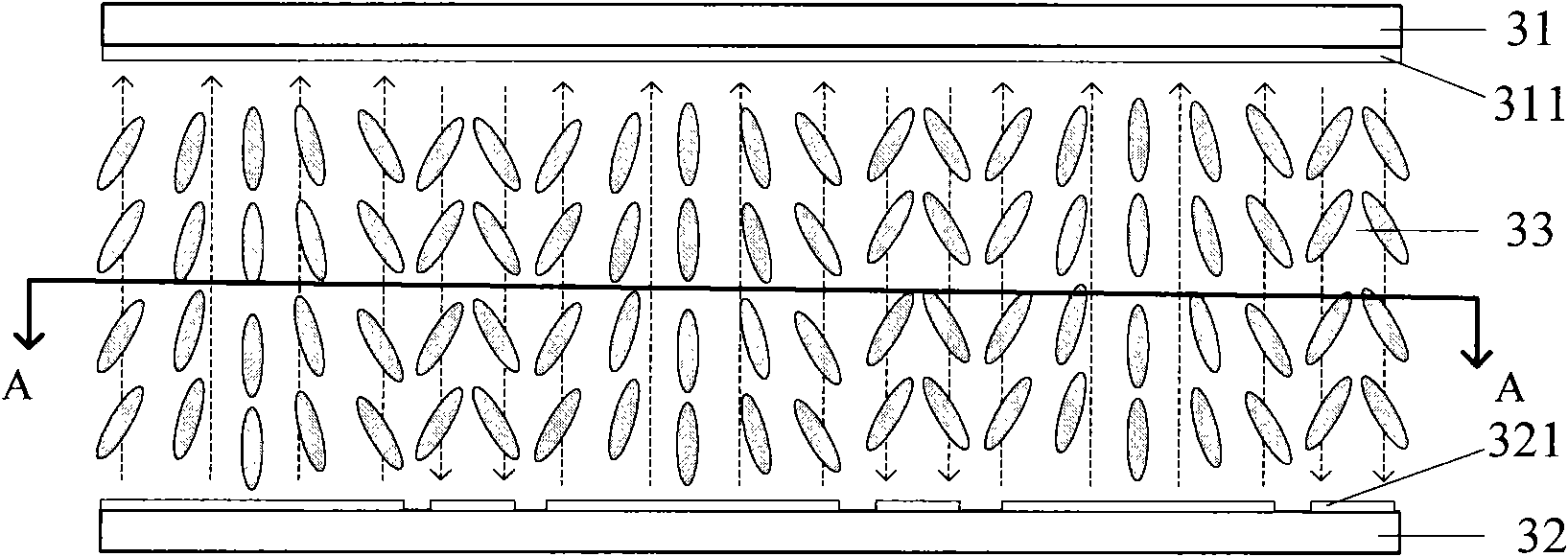
[0067] Please also see image 3 and Figure 4 , in this embodiment, the liquid crystal display panel includes a first substrate 31 and a second substrate 32 opposite to the first substrate 31 , and liquid crystal molecules 33 are sandwiched between the first substrate 31 and the second substrate 32 . In this embodiment, the first substrate 31 may be a color filter substrate, the second substrate 32 may be a thin film transistor array substrate, and the liquid crystal molecules 33 may be negative liquid crystal molecules, which are aligned vertically to the two substrates 31 and 32 . Wherein, a transparent electrode layer 311 is provided on the side close to the liquid crystal molecules 33 on the first substrate 31, and a plurality of sub-pixel electrodes 321 are provided on the side close to the liquid crystal molecules 33 on the second substrate 32, and each sub-pixel electrode 321 corresponds to a sub-pixel.

[0068] Each sub-pixel electrode 321 includes a first region 41 ...

Embodiment 2

[0084] The liquid crystal display panel 91 adopts the liquid crystal display panel designed with double grid lines as described in the foregoing liquid crystal display panel embodiment, and its circuit design is as follows Figure 14 shown. The driving circuit 92 drives the liquid crystal panel 91 in a row inversion driving manner, so that the polarity of the voltage applied to each sub-pixel electrode of the liquid crystal display panel 91 relative to the transparent electrode layer of the first substrate is opposite to that of the adjacent sub-pixel electrode. The voltage polarity of the transparent electrode layer of the first substrate is opposite.

[0085] Specifically, the schematic diagram of the driving signal of the driving circuit driver 92 driving the liquid crystal display panel 91 is as follows: Figure 15 shown, see again Figure 14 , in the liquid crystal display panel 91 , the first subpixel electrode and the second subpixel electrode in each row of subpixel ...


PUM


Abstract

The invention provides a liquid crystal display panel and a liquid crystal display device. The liquid crystal display panel comprises a first substrate and a second substrate opposite to the first substrate; liquid crystal molecules are sandwiched between the first substrate and the second substrate; a transparent electrode layer is arranged on one side of the first substrate close to the liquid crystal molecules; a plurality of sub-pixel electrodes are arranged on one side of the second substrate close to the liquid crystal molecules; each sub-pixel electrode comprises a polygonal display area; at least two sides of display areas of adjacent sub-pixel electrodes are adjacent; each sub-pixel electrode and the transparent electrode layer form a liquid crystal capacitor; and the voltage polarity of each sub-pixel electrode relative to the transparent electrode layer of the first substrate is opposite to that of an adjacent sub-pixel electrode relative to the transparent electrode layer of the first substrate. By comparing the manufacturing process of the liquid crystal display panel with the prior art, manufacturing process steps are reduced, the product yield is high and the manufacturing cost is reduced.

Description

technical field [0001] The invention relates to the technical field of liquid crystal display, in particular to a liquid crystal display panel and a liquid crystal display device. Background technique [0002] A liquid crystal display (Liquid Crystal Display, LCD) is a very common display now, and it has the advantages of small size, light weight, power saving, low radiation, and easy portability. Among various display modes of liquid crystal displays, a vertical alignment (VA) display mode liquid crystal display is widely welcomed in the market due to its advantages such as high contrast ratio and wide viewing angle. [0003] In the LCD of VA display mode, vertically aligned (VA) liquid crystal molecules are vertically arranged in the liquid crystal layer in the liquid crystal cell relying on the surface riveting energy of the alignment film layer, when an electric field is applied to the ITO substrate on both sides of the liquid crystal cell The liquid crystal molecules i...

Claims


Application Information

Patent Timeline
Patent Type & Authority Applications(China)
IPC IPC(8): G02F1/1343G02F1/1362G02F1/1368G02F1/1335
Inventor 马骏罗熙曦李忠丽凌志华
Owner SHANGHAI TIANMA MICRO ELECTRONICS CO LTD
Why Eureka
Try Eureka