IGBT (Insulated Gate Bipolar Translator) device structure and preparation method thereof

A device structure and device technology, applied in the field of trench IGBT device structure and preparation, can solve problems such as poor anti-latch-up characteristics, narrow safe working area, and increased series resistance

Active Publication Date: 2011-05-25
STARPOWER SEMICON
View PDF4 Cites 1 Cited by
  • Summary
  • Abstract
  • Description
  • Claims
  • Application Information

AI Technical Summary

Problems solved by technology

[0003] However, the usual trench type IGBT has poor anti-latch-up characteristics, and the safe operating area (SOA) is also narrow. The reason is that if an additional The P+ deep well structure is used to prevent the latch-up caused by the parasitic NPN tube effect, and the protruding P+ deep well can easily pinch off the surrounding N- substrate with extremely low doping concentration, which will increase the series resistance of the parasitic JFET tube. This negates the advantage of trench devices over planar devices

Method used


Image

  • IGBT (Insulated Gate Bipolar Translator) device structure and preparation method thereof
  • IGBT (Insulated Gate Bipolar Translator) device structure and preparation method thereof
  • IGBT (Insulated Gate Bipolar Translator) device structure and preparation method thereof

Examples


preparation example Construction

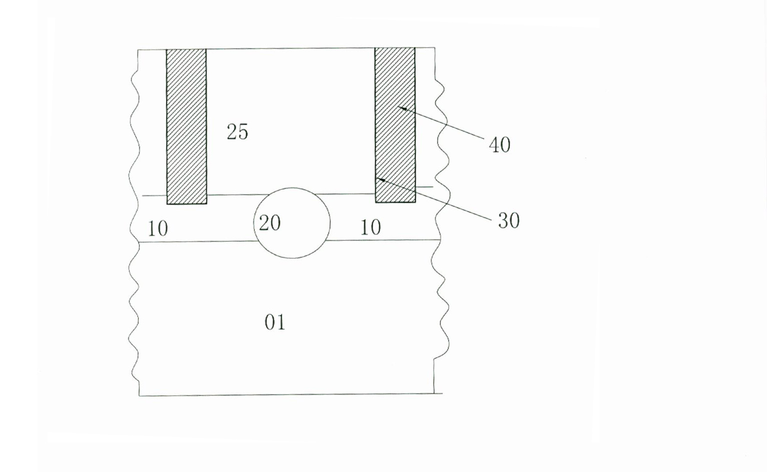
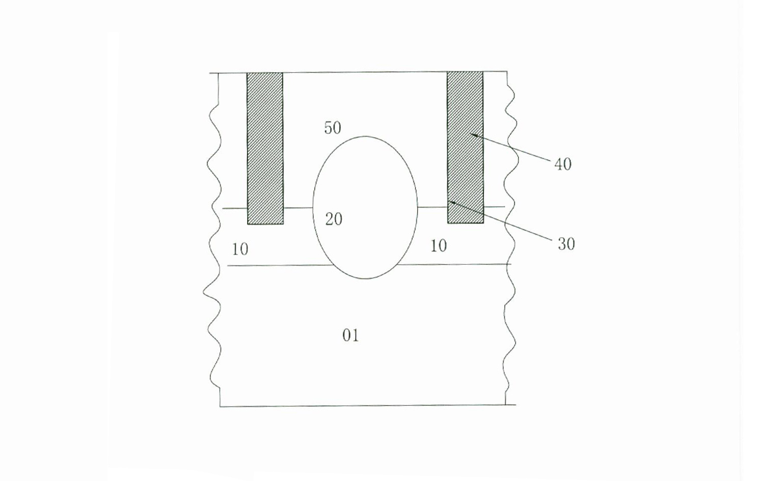
[0033] A method for preparing a trench type IGBT device structure with high latch-up resistance as described in the present invention, the preparation method includes the following steps: the first step is to provide a high-resistance N-type silicon substrate, and use the N-type Ion implantation introduces a medium-concentration N-type doped region (as an N-type well) with a higher concentration than the substrate in the device active region of the silicon substrate, and carries out high-temperature diffusion advancement; the second step, using a photolithography mask and boron Ion implantation introduces higher-doped P-type regions into the above-mentioned N-type wells at intervals as P-type deep wells, and anneals to activate; the third step is to grow a certain thickness of high-resistivity N-type epitaxial silicon on the silicon substrate by epitaxy. The fourth step is to use photolithography and etching technology to etch deep trench arrays in the active area of ​​the ...

Embodiment

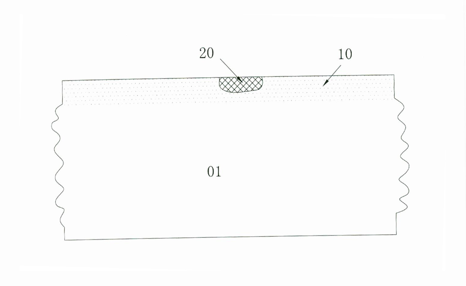
[0040] Example: see figure 1 , the first step and the second step of a manufacturing method of a highly latch-up resistant trench IGBT device with a P+ deep well of the present invention, on an N-type high-resistivity region melting type or epitaxial silicon substrate 01, using N-type ion implantation introduces a medium-concentration N-type doped region higher than the substrate concentration in the device active region of the silicon substrate. The impurity is usually phosphorus or arsenic, and the implantation dose is 5e11 / cm 2 to 5e13 / cm 2 The implantation energy is between 25keV and 1MeV; then carry out high-temperature diffusion and advance to form an N-type deep well 10; use a photolithography mask and boron ion implantation to introduce a P-type highly doped buried layer at intervals in the above-mentioned N-type doped region area, the boron ion implantation dose is 5e13 / cm 2 up to 1e15 / cm 2 Between, the implantation energy is between 30keV and 1MeV, and annealing i...


PUM


Abstract

The invention provides an IGBT (Insulated Gate Bipolar Translator) device structure which comprises an N type high resistance rate region melting type or epitaxial silicon substrate formed on a silicon base plate. An N type doping region with a medium concentration which is higher than the concentration of the substrate, a P type well, an N type epitaxial silicon layer and a grate zone of an MOS (Metal Oxide Semiconductor) structure are introduced in an active region of the device with the silicon substrate. P type doping and impurity diffusion are carried out on the epitaxial silicon layer between grooves at a depth part close to the bottoms of the grooves so as to form a P type MOS well region. Contact holes are etched in a transmitting region and a polysilicon gate zone, metal is deposited, and ohmic contact is formed between the metal, silicon and a polysilicon highly-doped region. The invention also provides a preparation method of the IGBT (Insulated Gate Bipolar Translator) device structure. The preparation method comprises the following steps of high temperature diffusion propulsion, annealing, activation and the like.

Description

technical field [0001] The invention relates to a trench type IGBT device structure and preparation method with high anti-latch characteristics, which belongs to the semiconductor manufacturing process. Background technique [0002] The trench IGBT device is an advanced IGBT device type, which moves the MOS control structure from the silicon surface to the vertical channel, and eliminates the parasitic JFET effect of the planar IGBT device, so that it can achieve the same device current capability. Under the same process cost, the device area can be reduced, and the cost performance of the device can be improved. [0003] However, the usual trench type IGBT has poor anti-latch-up characteristics, and the safe operating area (SOA) is also narrow. The reason is that if an additional The P+ deep well structure is used to prevent the latch-up caused by the parasitic NPN tube effect, and the protruding P+ deep well can easily pinch off the surrounding N- substrate with extremely...

Claims


Application Information

Patent Timeline
Patent Type & Authority Applications(China)
IPC IPC(8): H01L29/739H01L29/06H01L21/331
Inventor 沈华
Owner STARPOWER SEMICON
Why Eureka
Try Eureka