Semiconductor power device

A technology for power devices and semiconductors, applied in semiconductor devices, electrical components, circuits, etc., can solve problems such as increasing on-state voltage drop, reducing transconductance, and increasing on-state power loss.

Active Publication Date: 2012-10-31
BYD SEMICON CO LTD
View PDF6 Cites 2 Cited by
  • Summary
  • Abstract
  • Description
  • Claims
  • Application Information

AI Technical Summary

Problems solved by technology

However, increasing the doping concentration of the well region will lead to a significant increase in the surface concentration, thereby increasing the threshold voltage; at the same time, the diffusion of the deep junction well region will inevitably lead to an increase in lateral diffusion, a significant increase in the channel length, and a decrease in transconductance. state voltage drop, increasing on-state power loss

Method used


Image

  • Semiconductor power device
  • Semiconductor power device
  • Semiconductor power device

Examples


Embodiment 1

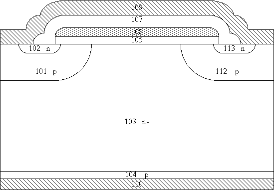
[0031] like figure 2 As shown, it is an n-channel IGBT of a semiconductor power device according to an embodiment of the present invention. The IGBT includes an n-type drift region 203. The drift region can be uniformly doped in a single layer or multi-layer doped. The drift region in this embodiment is The single layer is uniformly doped, and its doping concentration is; the p-type first well region 201 formed in a part of the n-type drift region 203, and its preferred doping concentration is; and the p-type well region separated from the first well region Type second well region 212, its preferred doping concentration is; the first source region 202 formed in a part of the first well region 201, its preferred doping concentration is; set the n-type second well region in the p second well region Source region 213, the preferred doping concentration is; wherein the forbidden band width of the well region is greater than the forbidden band width of the source region, and the e...

Embodiment 2

[0034] like Figure 4 As shown, it is a p-channel IGBT according to the embodiment of the present invention. The IGBT includes a p-type drift region 403 with a preferred doping concentration of . The drift region can be single-layer doped or multi-layer doped. In this embodiment, The drift region is uniformly doped in a single layer; the n-type first well region 401 formed in a part of the p-type drift region 403 has a preferred doping concentration of , and a second well separated from the first well region Region 412, its preferred doping concentration is; the p-type first source region 402 formed in a part of the first well region 401, its preferred doping concentration is, the first source region 402 disposed in the second conductivity type second well region 412 A conductivity type second source region 413; its preferred doping concentration is; wherein the forbidden band width of the well region is greater than the forbidden band width of the source region, the electron ...

Embodiment 3

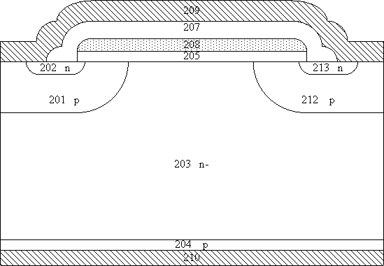
[0037] Image 6 is another embodiment of the present invention n-channel IGBT, it is with figure 2 The difference is that a barrier layer n-type 611 surrounding the well region is added on the surface of the n-type drift region. The doping concentration is all, the preferred material of the barrier layer in this embodiment is SiC, and the preferred material of the drift region is Si 1-x Gex, the barrier layer can cover the entire upper surface of the drift region, and of course the barrier layer can only cover part of the upper surface of the drift region.

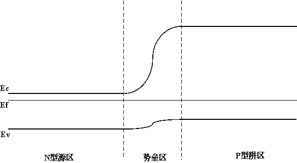
[0038] Figure 7 for Image 6 The schematic diagram of the energy band structure of the n-channel IGBT barrier layer and the drift region is shown. Since this embodiment is an n-channel IGBT, the minority carriers are holes, so the barrier layer is a hole barrier layer. It can be seen from the figure that the drift The Fermi level of the hole blocking layer is equal to that of the hole blocking layer; the conduction b...


PUM


Abstract

The invention relates to a power device, in particular to a semiconductor power device. The semiconductor power device comprises a first conducting type first semiconductor layer, a second conducting type well region arranged in the first semiconductor layer, a first conducting type source region arranged in the second conducting type well region, a first insulating layer which is arranged on the first semiconductor layer and covers the well region and the source region, a polysilicon layer positioned on the first insulating layer, a second insulating layer which is arranged on the polysilicon layer and covers the source region and the drain region, a first metal layer which covers the second insulating layer and is connected with the well region and the source region, a second conducting type second semiconductor layer positioned on the back surface of the first semiconductor layer and a second metal layer connected with the second semiconductor layer, wherein the forbidden band width of the well region is larger than the forbidden band width of the source region. The semiconductor disclosed by the invention has the advantages of improving the anti-latching capability of the semiconductor power device and increasing the breakover power consumption of the semiconductor power device.

Description

technical field [0001] The invention relates to a power device, especially a semiconductor power device. Background technique [0002] Semiconductor power devices have the advantages of high operating frequency, low conduction voltage, simple control circuit, and good reliability. Therefore, semiconductor power devices are widely used in the field of power control. like figure 1 It is a structural diagram of a typical n-type channel planar semiconductor power device, in which 101 is a p-type first well region, 112 is a p-type second well region, 102 is an n-type first source region, and 113 is an n-type second source region , 103 is an n-type drift region, 104 is a p-type collector region, 105 and 107 are insulating layers, 108 is a gate-level polysilicon, that is, a gate; 109 is a metal electrode, which is in contact with 101 and 102 ohms to form an emission Pole, 110 and 104 ohm contacts form the collector. [0003] Below the gate polysilicon 105, part of the surface be...

Claims


Application Information

Patent Timeline
Patent Type & Authority Applications(China)
IPC IPC(8): H01L29/06H01L29/739
Inventor 肖秀光王军鹤
Owner BYD SEMICON CO LTD
Why Eureka
Try Eureka