IGBT device and manufacturing method thereof

A device and substrate technology, applied in the field of IGBT devices and their fabrication, can solve problems such as burnout and breakdown of IGBT devices, and achieve the effects of reducing the rate of change, increasing the Miller capacitance, and improving the ability to resist latch-up.

Active Publication Date: 2017-05-24
JIANGSU CAS IGBT TECHNOLOGY CO LTD
View PDF6 Cites 2 Cited by
  • Summary
  • Abstract
  • Description
  • Claims
  • Application Information

AI Technical Summary

Problems solved by technology

[0005] In view of this, the present invention provides an IGBT device and a manufacturing method thereof, so as to improve the latch-up resistance of the IGBT device and solve problems such as breakdown and burnout of the IGBT device caused by the latch-up effect

Method used


Image

  • IGBT device and manufacturing method thereof
  • IGBT device and manufacturing method thereof
  • IGBT device and manufacturing method thereof

Examples


Embodiment Construction

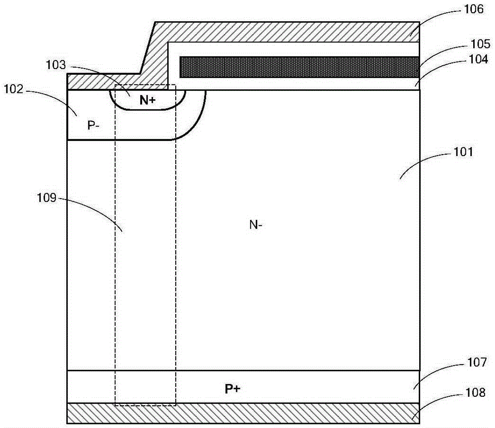
[0032] As mentioned in the background technology, there will inevitably be parasitic thyristors in the structure of the IGBT device, so that the voltage borne by the IGBT device will rise and fall rapidly in a short period of time during the turn-on and turn-off process, even if the voltage has a high change Rate. When the rate of change of the voltage is large enough, the parasitic thyristor may be triggered, so that the IGBT device is no longer controlled by the gate, causing a latch-up effect, which in turn leads to problems such as breakdown and burnout of the IGBT device.

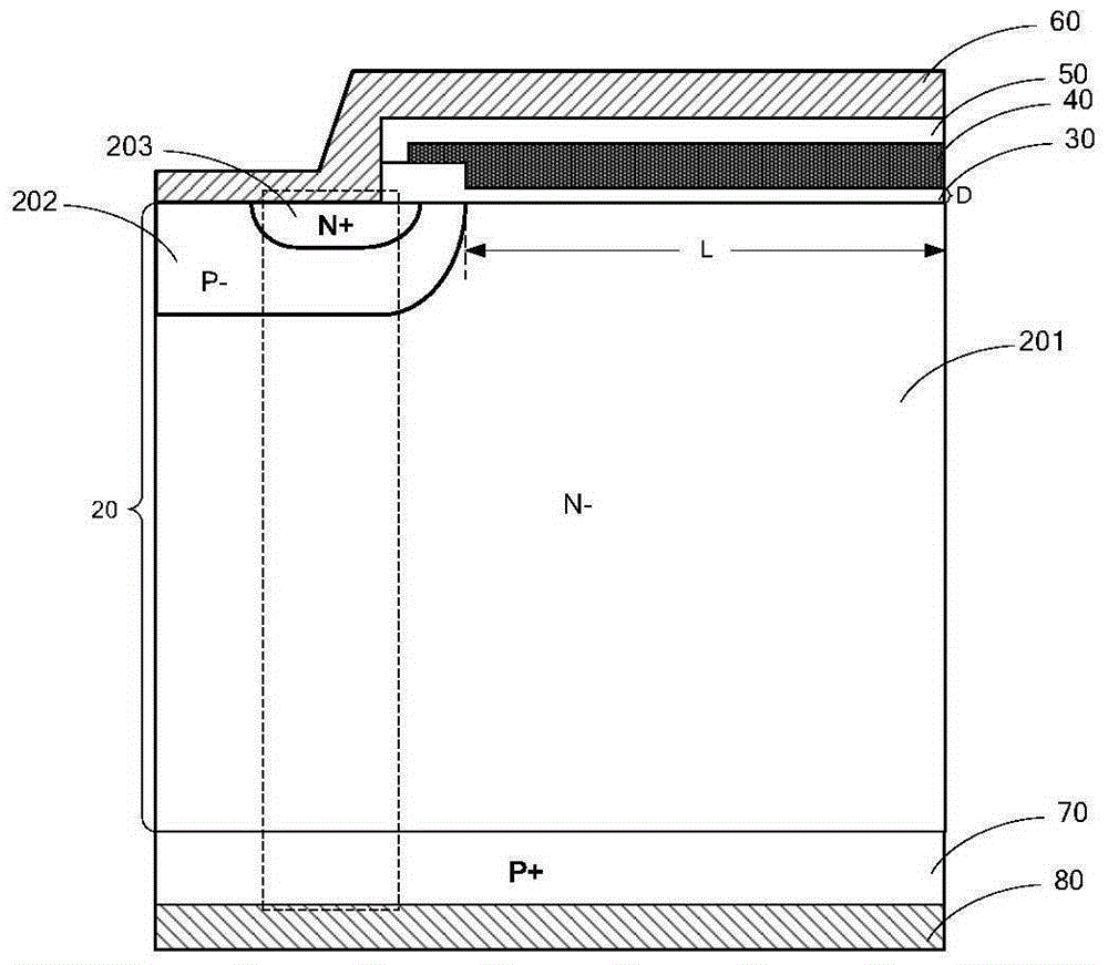
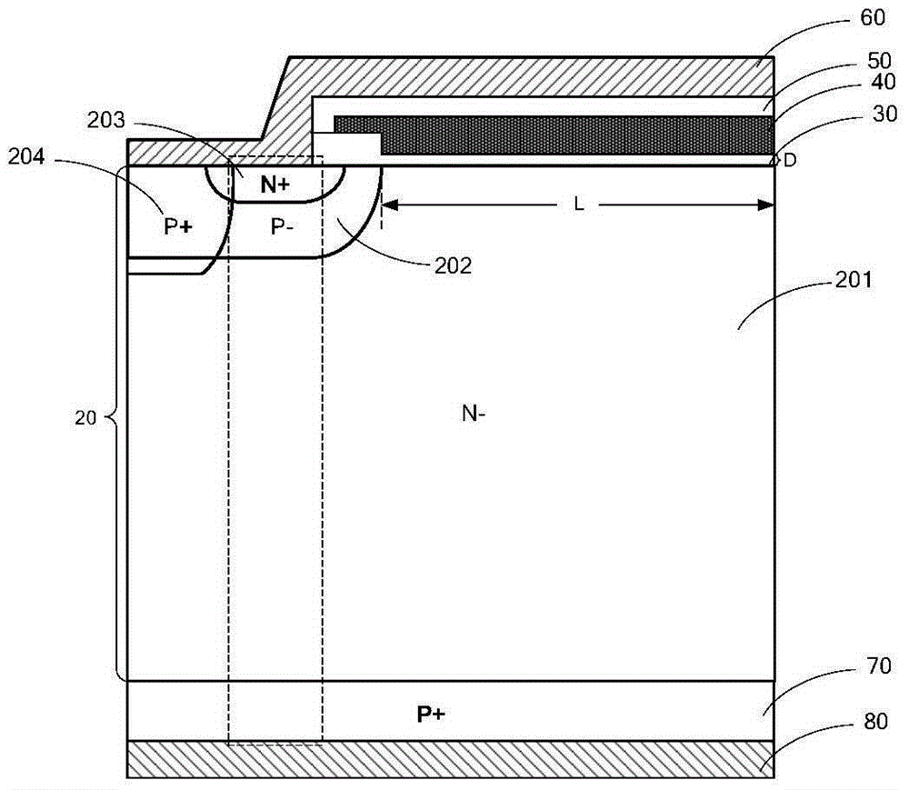
[0033] Based on this, the present invention provides an IGBT device and a manufacturing method thereof to overcome the above-mentioned problems in the prior art, including:

[0034] A substrate, the substrate includes a body layer, a well region and a source region located in the surface of the body layer; a first dielectric layer located on the front side of the substrate and a gate located on the sur...


PUM


Abstract

The invention provides an IGBT device and a manufacturing method thereof. The IGBT device comprises a substrate, a first dielectric layer, a grid electrode, a second dielectric layer and an emitter electrode; the substrate comprises a body layer and well and source regions positioned in the surface of the body layer; the first dielectric layer is positioned in the front side of the substrate; the grid electrode is positioned in the surface of the first dielectric layer; the thickness of the first dielectric layer between the grid electrode and the body layer ranges from 1nm to 100nm; the second dielectric layer is positioned in the surface of the grid electrode; and the emitter electrode is positioned in the front side of the second dielectric layer and the substrate. Due to the thickness of the first dielectric layer between the grid electrode and the body layer is limited in the range from 1nm to 100nm, the distance of Miller capacitance between the grid electrode and a collector electrode at the back side of the substrate is reduced, the Miller capacitance is increased, the voltage change rate born by the IGBT in the ON / OFF process is reduced, and the anti-latch-up capability of the IGBT device is improved.

Description

technical field [0001] The present invention relates to the technical field of semiconductors, and more specifically, relates to an IGBT device and a manufacturing method thereof. Background technique [0002] IGBT (Insulated Gate Bipolar Transistor, Insulated Gate Bipolar Transistor) is a composite fully-controlled voltage-driven power semiconductor device composed of a bipolar transistor and an insulated gate field effect transistor. Because the IGBT has the advantages of low driving power and low saturation voltage, the IGBT, as a new type of power electronic device, has been widely used in various fields. [0003] The structure of the existing IGBT device, taking the N-type channel as an example, such as figure 1 As shown, it includes: an N-type lightly doped (N-) substrate 101 and a gate dielectric layer 104 and a gate 105 on its front surface; a P-type well region 102 (generally a P-type light Doping), the N-type source region 103 located in the surface of the P-type...

Claims


Application Information

Patent Timeline
Patent Type & Authority Applications(China)
IPC IPC(8): H01L29/739H01L21/331H01L29/423
CPCH01L29/42364H01L29/66325H01L29/7393
Inventor 滕渊朱阳军卢烁今田晓丽
Owner JIANGSU CAS IGBT TECHNOLOGY CO LTD
Why Eureka
Try Eureka