Optical sensing module

A technology of optical sensing and optical sensor, which is applied in the direction of instruments, electrical digital data processing, input/output process of data processing, etc., and can solve the problems such as not easy to thin

Inactive Publication Date: 2012-07-25
AU OPTRONICS CORP
View PDF6 Cites 0 Cited by
  • Summary
  • Abstract
  • Description
  • Claims
  • Application Information

AI Technical Summary

Problems solved by technology

[0003] However, in the known optical finger navigation modules, image sensors (such as complementary metal oxide semiconductor image sensors) are mostly opaque chips, and generally need to be equipped with a lens to capture a good finger image. The arrangement of the image sensor and the lens makes the known optical finger navigation modules all have a certain thickness and volume, which is not easy to be thinned
For example, optical finger navigation modules disclosed in US Patent No. 7,045,775, US Patent No. 7,161,682, US Patent No. 6,433,780, US Patent No. 5,686,720, US Patent No. 7,408,718, and US Patent Publication No. Disadvantages of difficulty in thinning

Method used


Image

  • Optical sensing module
  • Optical sensing module
  • Optical sensing module

Examples


no. 1 example

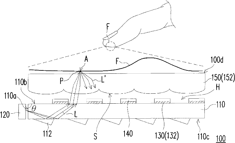
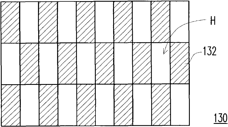
[0040] figure 1 It is a schematic cross-sectional view of the optical sensing module according to the first embodiment of the present invention. Please refer to figure 1 , the optical sensing module 100 of this embodiment may include a light guide 110 , a light source 120 , a light shielding element 130 , a plurality of light sensors 140 and an optical element 150 . The light conducting element 110 has a light incident surface 110a and a light exit surface 110b, and an included angle θ exists between the light incident surface 110a and the light exit surface 110b. In detail, the light incident surface 110a and the light exit surface 110b can be connected, and there is an included angle θ between the light incident surface 110a and the light exit surface 110b, and the included angle θ is, for example, 90°. However, the present invention is not limited thereto, and the angle θ between the light-incident surface 110 a and the light-exit surface 110 b can be designed differently...

no. 2 example

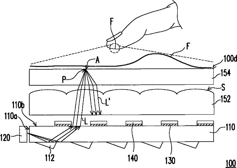
[0052] Image 6 It is a schematic cross-sectional view of the optical sensing module 300 according to the second embodiment of the present invention. The optical sensing module 300 of this embodiment is similar to the optical sensing module 100 of the first embodiment, and only the differences between the two will be described below, and the similarities will not be repeated.

[0053] Please refer to Image 6 , the optical sensing module 300 of this embodiment includes a light-conducting element 110 , a light source 120 , a light-shielding element 130 , a plurality of light sensors 140 and an optical element 150 . The light conducting element 110 has a light incident surface 110a and a light exit surface 110b, and an included angle θ exists between the light incident surface 110a and the light exit surface 110b. The light source 120 is adapted to provide light L, and the light L enters the light-conducting member 110 from the light-incident surface 110a, and exits the light-...


PUM


Abstract

The invention discloses an optical sensing module, which comprises a light conducting element, a light source, a light blocking element, a plurality of optical sensors and optical elements.The light conducting element has a plane of light incidence and a plane of emitting light and the light source provides light.The light blocking element is arranged on a portion of the plane of emitting light and the plurality of optical sensors are arranged on the light blocking element.The optical elements are arranged above the plane of emitting light.The optical sensors and the light blocking element are arranged between the optical elements and the light conducting element.The optical elements have touch surfaces.Light discharged out of the plane of emitting light passes through the optical elements.When an object touches the touch surface, the light is reflected and is received by the optical sensors.

Description

technical field [0001] The present invention relates to an optical sensing module, and in particular to a thinned optical sensing module. Background technique [0002] With the rapid development and application of information technology, wireless mobile communication and information home appliances, many information products, such as smart phones, notebook computers, etc., are equipped with optical finger navigation modules (optical finger navigation, OFN). In the known optical finger navigation modules, most infrared light emitting diodes are used as light sources, and the infrared light emitted by the infrared light emitting diodes is projected onto the user's finger through a prism, and the image of the finger is passed through an image sensor (such as a complementary metal oxide object semiconductor image sensor) capture. Then, after the image of the finger is captured by the image sensor, an image processing method can be used to analyze the differences of the images ...

Claims


Application Information

Patent Timeline
Patent Type & Authority Patents(China)
IPC IPC(8): G06F3/042
Inventor 王炯翰
Owner AU OPTRONICS CORP
Why Eureka
Try Eureka