Flash memory wear balance method

A technology of wear leveling and dynamic wear leveling, which is applied in the direction of memory system, memory architecture access/allocation, memory address/allocation/relocation, etc. It can solve the problems affecting the read and write performance of the wear leveling algorithm system and improve the read and write performance and longevity effects

Active Publication Date: 2011-06-01
HUAZHONG UNIV OF SCI & TECH
View PDF2 Cites 74 Cited by
  • Summary
  • Abstract
  • Description
  • Claims
  • Application Information

AI Technical Summary

Problems solved by technology

In an environment where the capacity of flash memory chips is gradually increasing, the existing wear leveling algorithm is already suffering from scalability problems, which seriously affects the income of the wear leveling algorithm and the read and write performance of the system.

Method used


Image

  • Flash memory wear balance method
  • Flash memory wear balance method
  • Flash memory wear balance method

Examples


Embodiment Construction

[0069] The technical solutions in the embodiments of the present invention will be clearly and completely described below in conjunction with the drawings in the embodiments of the present invention.

[0070] The wear leveling method of a kind of flash memory of the present invention adopts the method for dividing and conquering to flash memory (as solid state disk), specifically comprises the following steps:

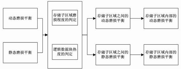
[0071] The total storage area is divided into N storage sub-areas, and two levels of dynamic / static wear balance are implemented for the interior of the storage sub-area and the storage sub-area.

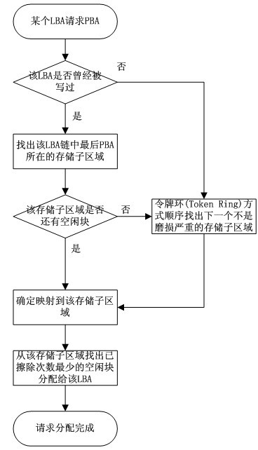
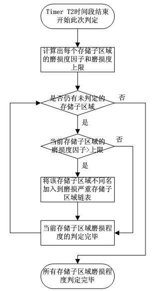
[0072] The system maintains an erased count table (Erase Count Table), which records the number of erased times of all physical blocks in the storage system. If a physical block is erased once, the data item corresponding to the physical block plus 1.

[0073] The system checks the wear condition of each physical block through the statistics table of the number of times era...


PUM


Abstract

The invention discloses a flash memory wear balance method, which comprises the following steps of: (1) dividing a flash memory storage area into a plurality of storage subareas; (2) determining the wear degree of various storage subareas at intervals, numbering seriously worn storage subareas, and interposing the seriously worn storage subareas into a seriously worn storage subarea queue; and (3) performing a dynamic wear balance operation to achieve flash memory wear balance when a logic block requires a newly allocated physical block. The wear balance method is suitable for performing the wear balance on memory devices such as flash memories, is not affected by the extensibility problem, is also suitable for large-capacity flash memory devices, and can greatly improve the read-write performance and the service life of memory systems.

Description

technical field [0001] The invention belongs to the field of semiconductor storage, and in particular relates to a wear leveling method of a flash memory. Background technique [0002] Flash memory is more and more widely used in various fields because of its high density, large capacity, low time-consuming read and write operations, low energy consumption, and non-volatility; at the same time, some of the flash memory chips themselves Defects limit the applications of this type of memory. First, the writing operation of the flash memory must be performed in a blank area. If there is data in the target area, it must be erased first and then written. The flash memory is erased in units of blocks. Second, the number of erasable times of a flash memory chip is limited. The number of erasable times for NOR flash memory is generally about 100,000 times, and the number of erasable times for NAND flash memory is generally about one million times. [0003] However, in the actual u...

Claims


Application Information

Patent Timeline
Patent Type & Authority Applications(China)
IPC IPC(8): G06F12/02
CPCG06F12/0246G06F2212/7211
Inventor 刘景宁冯丹童薇项南胡洋秦亦
Owner HUAZHONG UNIV OF SCI & TECH
Why Eureka
Try Eureka