Method for processing back surface of wafer

A backside processing and wafer technology, applied in the direction of electrical components, semiconductor/solid-state device manufacturing, circuits, etc., can solve the problems of poor metallization quality and easy peeling of the metal layer, so as to improve the quality, improve the quality of the backside surface, and ensure reliability sexual effect

Inactive Publication Date: 2011-06-01
PEKING UNIV FOUNDER GRP CO LTD +1
View PDF0 Cites 27 Cited by
  • Summary
  • Abstract
  • Description
  • Claims
  • Application Information

AI Technical Summary

Problems solved by technology

[0005] The embodiment of the present invention provides a wafer back processing method to solve the problems of poor back metallization quality and easy peeling of the metal layer existing in the prior art

Method used


Image

  • Method for processing back surface of wafer
  • Method for processing back surface of wafer
  • Method for processing back surface of wafer

Examples


Embodiment Construction

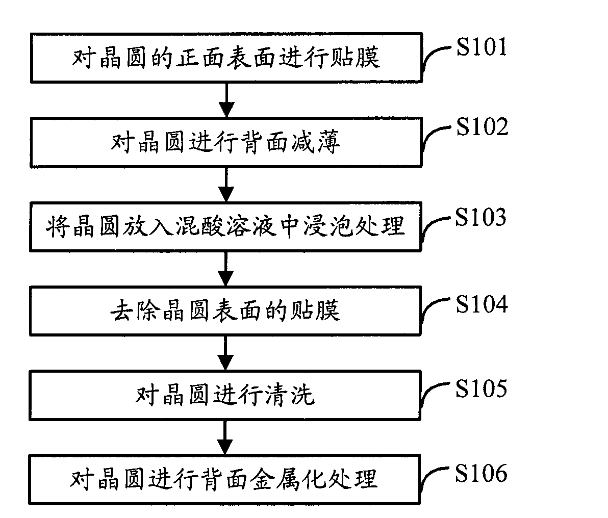
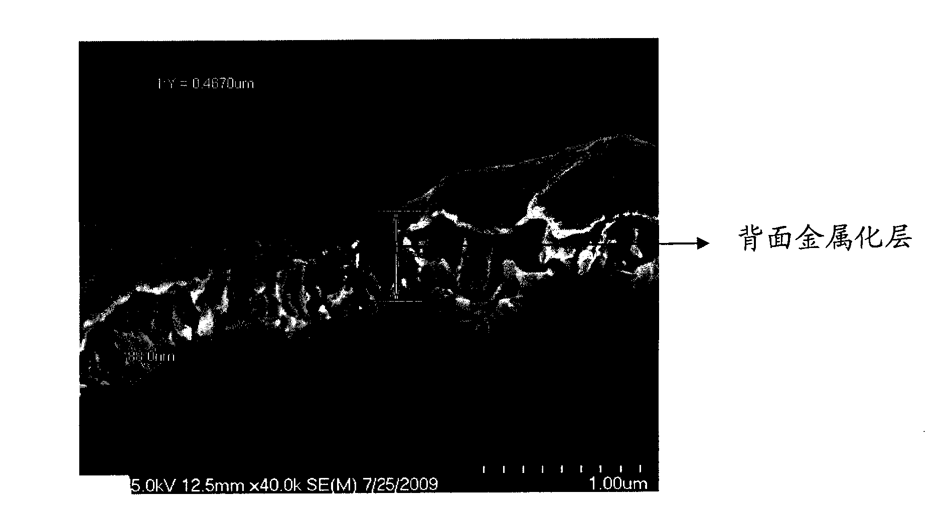
[0032] In order to improve the poor quality of the metallization layer on the back of the wafer in the prior art, and the problem that warping and deformation are prone to occur, the method for processing the back of the wafer provided by the embodiment of the present invention mainly involves the post-processing of the wafer. The thinning of the section processing technology, the improvement of the back gold and other related technological processes, the process is as follows figure 1 As shown, the execution steps are as follows:

[0033] Step S101: Applying a film to the front surface of the wafer.

[0034] The purpose of attaching the film to the front surface of the wafer is to protect the semiconductor devices on the front surface of the wafer from damage during subsequent processing.

[0035] Generally, a layer of acid-resistant blue film can be pasted on the front surface of the wafer. Apply film to the front surface of the wafer through a dedicated film mounter, for ...


PUM


Abstract

The invention discloses a method for processing a back surface of a wafer, and the method is applied to the manufacturing process of a semiconductor wafer. The method comprises: thinning the back surface of the wafer to obtain a thinned wafer; placing the wafer in a mixed acid solution with a set proportion for soaking according to the surface quality of the back surface of the thinned wafer so as to acquire the surface quality satisfying the back surface metallization requirement; and carrying out back surface metallization processing on the wafer after cleaning the soaked wafer, and coating a required metal layer on the back surface of the wafer. According to the method disclosed by the invention, the surface quality of the back surface of the wafer is improved through soaking by the mixed acid, so that the warping, curling and flaking of the metallization layer of the back surface can not happen.

Description

technical field [0001] The invention relates to the technical field of semiconductor manufacturing technology, in particular to a wafer backside processing method used in the semiconductor wafer manufacturing process. Background technique [0002] At present, metal-oxide-semiconductor (Metal Oxide Semiconductor, MOS) field-effect transistors, referred to as MOS transistors, and other devices using ultra-thin chips have been widely used in the semiconductor field, especially in smart cards, radio frequency identification (Radio Frequency Identification (RFID) devices, new mobile phones, personal digital assistants (Personal Digital Assistant, PDA) and other small, light and powerful electronic devices are more widely used. [0003] In the manufacturing process of ultra-thin chips, the back-end process of wafer processing generally includes: film-back thinning-film removal-cleaning-back gold (back metallization) and other process steps, of which the back side thinning and clea...

Claims


Application Information

Patent Timeline
Patent Type & Authority Applications(China)
IPC IPC(8): H01L21/00H01L21/60H01L21/306
Inventor 李熙胡德明
Owner PEKING UNIV FOUNDER GRP CO LTD
Why Eureka
Try Eureka