Method for manufacturing semiconductor device having buried gate

A buried, gate conductive layer technology, used in semiconductor/solid-state device manufacturing, semiconductor devices, electrical solid-state devices, etc.

Active Publication Date: 2011-06-15
SK HYNIX INC
View PDF4 Cites 20 Cited by
  • Summary
  • Abstract
  • Description
  • Claims
  • Application Information

AI Technical Summary

Problems solved by technology

[0009] However, according to the prior art described above, a polysilicon portion for forming a bit line in the cell region and a portion of polysilicon for forming a gate in the core / peripheral region are excessively deposited near the boundary portion between the cell region and the core / peripheral region. another polysilicon portion of the pole, unexpectedly encountering various problems when removing the over-deposited polysilicon portion

Method used


Image

  • Method for manufacturing semiconductor device having buried gate
  • Method for manufacturing semiconductor device having buried gate
  • Method for manufacturing semiconductor device having buried gate

Examples


Embodiment Construction

[0027] As required, detailed embodiments of the invention are disclosed herein. However, it is to be understood that the disclosed embodiments are merely examples of the invention, and that the invention can be embodied in various forms. Therefore, specific details disclosed herein are not to be interpreted as limiting, but merely as a basis for the claims and as a representative basis for teaching one skilled in the art to employ the present invention in virtually any suitable manner.

[0028] Reference will now be made in detail to the embodiments of the invention, examples of which are illustrated in the accompanying drawings. Wherever possible, the same reference numbers will be used throughout the drawings to refer to the same or like parts.

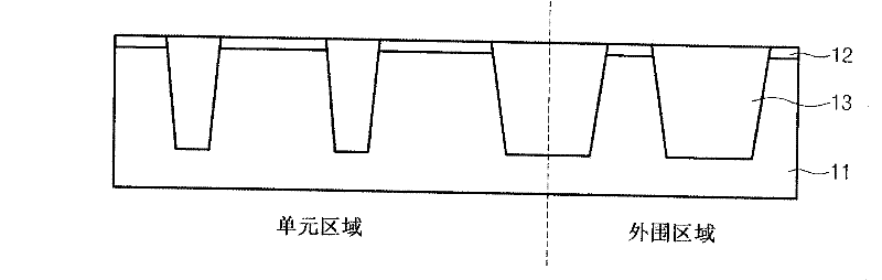
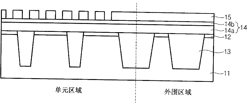
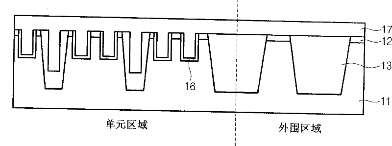
[0029] Figure 1 to Figure 11 is a cross-sectional view showing a semiconductor device including a buried gate according to an embodiment of the present invention.

[0030] refer to figure 1 , a pad oxide layer (not shown) and a...


PUM


Abstract

A method for manufacturing a semiconductor device having a buried gate is provided. A gate conductive layer is first formed in the peri region before a bit line contact is formed in the cell region, so that a fabrication process is simplified and the problem caused by a step height between the cell region and the core / peri region is not encountered.

Description

technical field [0001] The present invention relates to a method of manufacturing a semiconductor device, and more particularly, to a method of manufacturing a semiconductor device that simplifies the manufacturing process of a semiconductor device having a buried gate and minimizes problems caused by the manufacturing process. Background technique [0002] As the integration level of semiconductor storage devices such as Dynamic Random Access Memory (DRAM) increases, the area occupied by Metal Oxide Semiconductor (MOS) transistors gradually decreases. Accordingly, the channel length of the MOS transistor is also reduced, so that a short channel effect occurs. Specifically, if a short channel effect occurs in an access MOS transistor in a memory unit (cell, also called a unit cell) used for DRAM, the threshold voltage of the DRAM cell decreases, and the leakage current of the DRAM cell increases , so the refresh characteristics of the DRAM are degraded. [0003] Therefore,...

Claims


Application Information

Patent Timeline
Patent Type & Authority Applications(China)
IPC IPC(8): H01L21/82H01L21/336H01L21/28H01L21/768H01L21/8242
CPCH01L27/10876H01L21/823431H01L27/10894H01L27/10888H10B12/053H10B12/485H10B12/09H01L21/108H01L21/2254H01L21/4763H01L29/42312H01L29/66348H10B12/482
Inventor 金永得
Owner SK HYNIX INC
Why Eureka
Try Eureka