Optical transceiver and manufacturing method thereof
一种光收发器、制造方法的技术,应用在光收发器及其制造领域,能够解决对位过程复杂、不利产品批量生产等问题,达到制程简单的效果
- Summary
- Abstract
- Description
- Claims
- Application Information
AI Technical Summary
Problems solved by technology
Method used
Image

Examples
Embodiment Construction
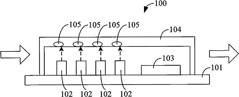
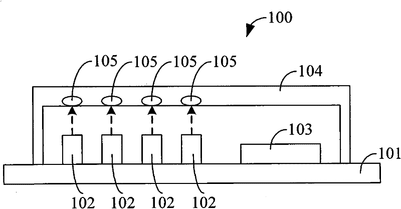
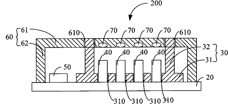
[0027] figure 2 Shown is a schematic diagram of the structure of the optical transceiver 200 of the present invention. In this embodiment, the optical transceiver 200 is used for photoelectric signal conversion, and includes a substrate 20 , a positioning seat 30 , a plurality of laser components 40 , a laser driver chip 50 , a bracket 60 and a plurality of lenses 70 .
[0028] The positioning seat 30 has a base 31 and a pair of positioning columns 32. The positioning columns 32 are arranged near the two ends of the base 31. The base 31 has a plurality of mounting holes 310 formed between the two positioning columns 32 for the precise installation of the laser element 40. Location. In this embodiment, the laser element 40 passes through the mounting hole 310 and is welded to the substrate 20 by wire bonding for sending and receiving photoelectric signals. Similarly, the laser driver chip 50 is also welded to the substrate 20 by wire bonding for driving the laser element 40 ....
PUM
 Abstract
Description
Claims
Application Information
 - R&D
- Intellectual Property
- Life Sciences
- Materials
- Tech Scout
- Unparalleled Data Quality
- Higher Quality Content
- 60% Fewer Hallucinations
Browse by: Latest US Patents, China's latest patents, Technical Efficacy Thesaurus, Application Domain, Technology Topic, Popular Technical Reports.
© 2025 PatSnap. All rights reserved.Legal|Privacy policy|Modern Slavery Act Transparency Statement|Sitemap|About US| Contact US: help@patsnap.com