A method for making L2 blind hole of high-density interconnection circuit board

A technology of high-density interconnection and second-order blind holes, which is applied to the removal of conductive materials by chemical/electrolytic methods, multilayer circuit manufacturing, printed circuit components, etc., can solve the problem of affecting the transmission effect of electrical signals between multilayer lines, Affecting the shape of second-order blind holes, many process steps, etc.

Inactive Publication Date: 2007-11-28
AVARY HLDG (SHENZHEN) CO LTD +1
View PDF0 Cites 31 Cited by
  • Summary
  • Abstract
  • Description
  • Claims
  • Application Information

AI Technical Summary

Problems solved by technology

[0005] However, in the manufacturing process of the above-mentioned second-order blind holes, both the first copper window and the second copper window are opened by chemical etching, which requires two processes of photoresist coating, exposure, development, and etching. There are many steps in this process, and each Some errors will inevitably be introduced in the steps, so that the position and size of the first copper window and the second copper window obtained will have errors, and the centers of the upper and lower holes of the second-order blind holes

Method used


Image

  • A method for making L2 blind hole of high-density interconnection circuit board
  • A method for making L2 blind hole of high-density interconnection circuit board
  • A method for making L2 blind hole of high-density interconnection circuit board

Examples


Embodiment Construction

[0023] The method for manufacturing second-order blind holes of a high-density interconnection circuit board will be further described in detail below with reference to the accompanying drawings and embodiments.

[0024] This embodiment provides a method for manufacturing a second-order blind hole of a high-density interconnection circuit board, which includes the following steps:

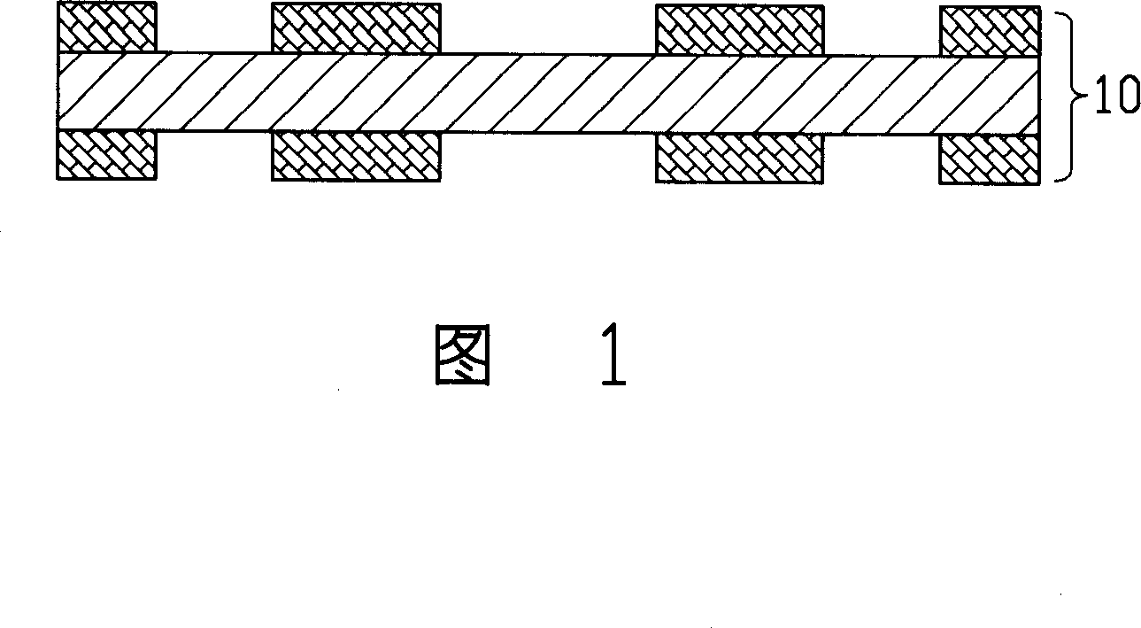
[0025] (a) providing a circuit board with a circuit on at least one side thereof;

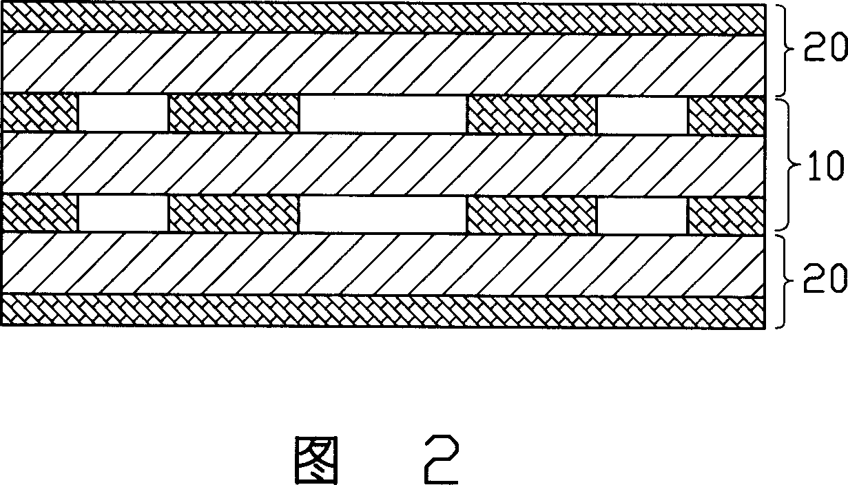
[0026] (b) forming a first adhesive-backed copper foil on the circuit surface;

[0027] (c) forming a plurality of first copper windows in the copper foil layer of the first adhesive-backed copper foil;

[0028] (d) forming a second adhesive copper foil on the surface of the first adhesive copper foil formed with the first copper window;

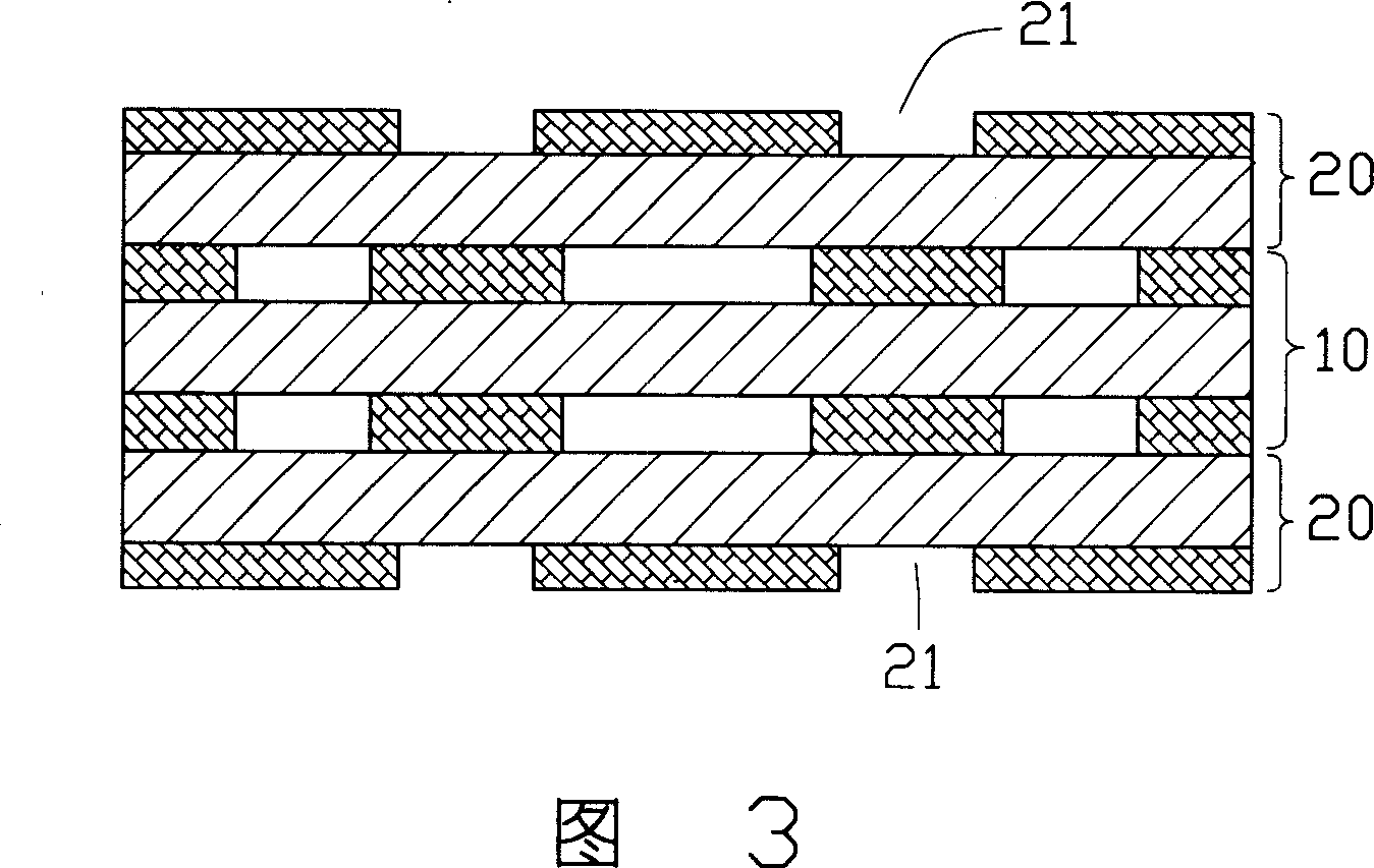
[0029] (e) using a first laser to form a plurality of second copper windows corresponding to the first copper windows in the copper foil layer of the second adhesive-backed copp...


PUM

PropertyMeasurementUnit
Wavelengthaaaaaaaaaa

Abstract

This invention relates to a method for processing second-order blind holes of high density interlinked CB including the following steps: providing a CB with a circuit on one side, forming a first back-glued copper foil on the surface of the circuit, forming multiple first copper windows in the copper foil layer, forming a second back-glue copper foil on the surface of the first copper foil with the first copper windows, utilizing a laser to open multiple second copper windows corresponding to the first ones in the layer of the second copper foil, utilizing a second laser to eliminate the subs of the two copper foils from the second copper windows so as to form multiple second-order blind holes.

Description

technical field [0001] The invention relates to a manufacturing technology of a multilayer circuit board, in particular to a method for manufacturing a second-order blind hole of a high-density interconnection circuit board. Background technique [0002] The expansion of the mobile phone market and the substantial increase in demand have led to the vitality of circuit boards. At present, the circuit boards used in mobile phones generally include traditional laminated boards and build-up multilayer (BUM) according to the process technology. . The BUM board is currently the highest-level process technology for manufacturing mobile phone circuit boards. That is, the outer layer of the double-sided or single-sided board is laminated with Resin Coated Copper Foil (RCC) and formed in a non-mechanical way. Holes (mostly micro-blind holes) become high-density interconnect (HighDensity Interconnect, HDI) circuit boards. HDI circuit boards usually refer to circuit boards that use mi...

Claims


Application Information

Patent Timeline
IPC IPC(8): H05K3/42H05K3/46H05K3/06H05K1/09
Inventor 李文钦林承贤
Owner AVARY HLDG (SHENZHEN) CO LTD
Why Eureka
Try Eureka