Manufacturing method of light-emitting diode

A technology of light-emitting diodes and manufacturing methods, applied in semiconductor/solid-state device manufacturing, electrical components, electric solid-state devices, etc., capable of solving problems such as increased risk of short-circuits in light-emitting diode wafers, and existing short circuits

Inactive Publication Date: 2011-06-22
HONG FU JIN PRECISION IND (SHENZHEN) CO LTD +1
View PDF2 Cites 5 Cited by
  • Summary
  • Abstract
  • Description
  • Claims
  • Application Information

AI Technical Summary

Problems solved by technology

However, since the light-emitting diode chips are arranged in a relatively dense array, when the light-emitting diode chips are pressed into the conductive glue, the conductive particles in the conductive glue will run to the adjacent light-emitting diodes due to being squeezed. In the gap between the diode chips, the adjacent light-emitting diode chips will be conducted due to th

Method used


Image

  • Manufacturing method of light-emitting diode
  • Manufacturing method of light-emitting diode
  • Manufacturing method of light-emitting diode

Examples


Embodiment Construction

[0020] see figure 1 , the manufacturing method of the light-emitting diode of the present invention comprises the following steps:

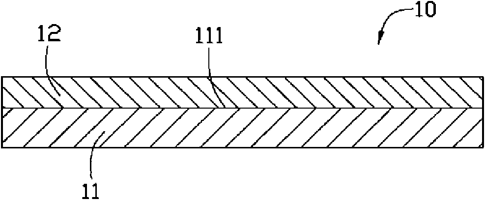
[0021] First, as figure 2 As shown, a light-emitting diode wafer 10 is provided. The LED chip 10 includes a substrate 11 and an epitaxial layer 12 grown on the substrate 11 . The material of the substrate 11 can be sapphire, silicon or silicon carbide. In this embodiment, the substrate 11 is sapphire, and the epitaxial layer 12 is grown upward from the upper surface 111 of the sapphire substrate 11 . The epitaxial layer 12 is a semiconductor forming a p-n junction, and the material of the epitaxial layer 12 can be gallium arsenide, gallium arsenide phosphide, aluminum gallium arsenide, or the like.

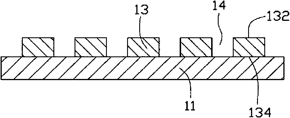
[0022] Second, if image 3 As shown, the epitaxial layer 12 of the LED wafer 10 is cut into a plurality of LED chips 13 . Each LED chip 13 includes a top surface 132 and a bottom surface 134 , and the bottom surface 134 of the LED chip 13 is cl...


PUM


Abstract

The invention relates to a manufacturing method of a light-emitting diode, comprising the following steps of: supplying a light-emitting diode wafer, wherein the light-emitting diode wafer comprises a base plate and an epitaxial layer grown from the base plate; cutting the epitaxial layer of the light-emitting diode wafer into a plurality of mutually separated light-emitting diode chips, wherein a gap is formed between adjacent light-emitting diode chips; arranging an insulating layer in the gap positioned between the adjacent light-emitting diode chips; supplying a bottom plate, wherein a conductive adhesive is coated on the bottom plate; inversing the base plate and the light-emitting diode chips so that each light-emitting diode chip is connected with the conductive adhesive of the bottom plate, wherein the insulating layer obstructs the conductive adhesive positioned between the adjacent light-emitting diode chips; and cladding the light-emitting diode wafer by utilizing a light-transmitting material so as to obtain the light-emitting diode.

Description

technical field [0001] The present invention relates to a manufacturing method of a light emitting diode. Background technique [0002] As an emerging third-generation light source, light-emitting diode light source is generally favored by the market because of its advantages of long working life, energy saving and environmental protection. Moreover, the current light-emitting module composed of light-emitting diodes can generate high-power, high-brightness light sources. Therefore, it will widely and revolutionaryly replace the existing light sources such as traditional white woven lamps, and become the main light source in line with the theme of energy saving and environmental protection. However, when manufacturing light-emitting diodes, most of the LED chips are first cut into a plurality of LED chip units, and then the plurality of LED chip units are placed on a base plate one by one, and then the LED chips are packaged in a single package. Single-body packaging into ...

Claims


Application Information

Patent Timeline
IPC IPC(8): H01L21/50H01L21/54H01L21/60H01L25/075H01L33/48
CPCH01L2224/83192H01L2224/16225H01L2224/32225H01L24/95H01L2224/73204H01L24/81H01L2924/12041H01L2924/00
Inventor 赖志成
Owner HONG FU JIN PRECISION IND (SHENZHEN) CO LTD
Why Eureka
Try Eureka