Array antenna of wide-band and low-profile beam wireless communication base station

An array antenna and wireless communication technology, which is applied in the direction of the separately powered antenna array, the radiating element structure, etc., can solve the problems of low antenna efficiency, lack of array antenna, and difficulty in obtaining more accurate beam width, etc., to improve performance, Wide impedance characteristics, light weight effect

Inactive Publication Date: 2011-06-29
XINGDONG COMM TECH SUZHOU
4 Cites 7 Cited by

AI-Extracted Technical Summary

Problems solved by technology

However, some array antennas cannot work in wireless communication systems such as GSM1800 (1710-1880MHz), CDMA1900 (1850-1990MHz) and ITU's IMT-2000 (1885-2170MHz); at the same time, because many array antennas do not have a symmetrical feeding structure, the antenna The efficiency is relatively low; in order to meet...

Method used

Referring to Fig. 2, the antenna includes 6 array units, and each array unit is excited with equal amplitude and same phase. The array spacing is 0.82λ0. If the width of the reflector is designed to be 0.55λ0, and two metal folds with a height of 0.128λ0 are added around it, after calculation, the beam width of the azimuth plane is close to 78° in the entire frequency band, which is about less than the specification The values ​​in 90±8° are less likely to achieve a more precise beamwidth of 90±2°. At this time, if the width of the reflector is narrowed, the beam width can be widened and develop towards the beam width specified in the specification, but at this time, the standing wave ratio and front-to-back ratio of the array antenna will also change, and it will deviate from the specified beam width. Direction of the specified value. In order to widen the beam width while keeping other characteristics unchanged, the present invention adopts a reflector with slotted metal folds. The width of the gap metal flange is 0.031λ0, the slot spacing is 0.069λ0, and the slot height is 0.128λ0. The slot is equivalent to an additional radiator re-excited by the excitation radiation patch and the parasitic radiation patch. The electric field at the observation point in the far zone is the vector superposition of the radiation field of the gap and the radiation field of the radiation patch. Since the input impedance of the radiation patch and the slit is different, the phase of the original electric field generated by the radiation patch and the slit is also different, and at the same time, the distance between the observation point in the far area and the radiation patch and the slit is also different, resulting in The phase difference is also different. In this way, the field at the observation point in the far zone is determined by the shape of the array unit and the shape of the reflector (including the folded edge of the slit). Under the condition that other characteristics have met the technical specifications, the beam width can be adjusted in a small range by changing the shape of the gap metal fold, so that it has a more precise beam width, while other characteristics...

Abstract

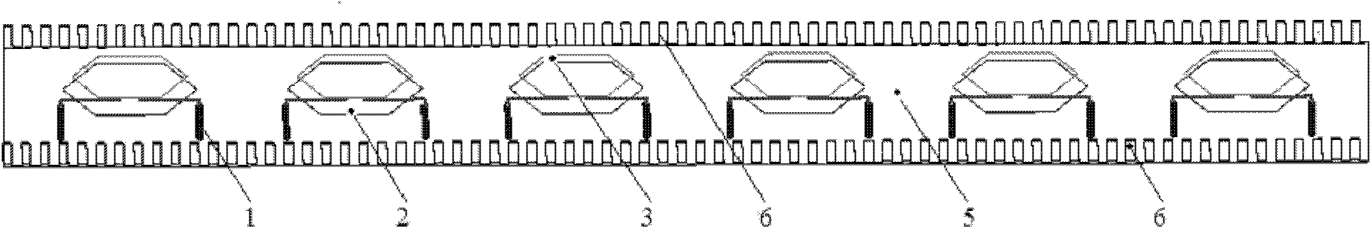
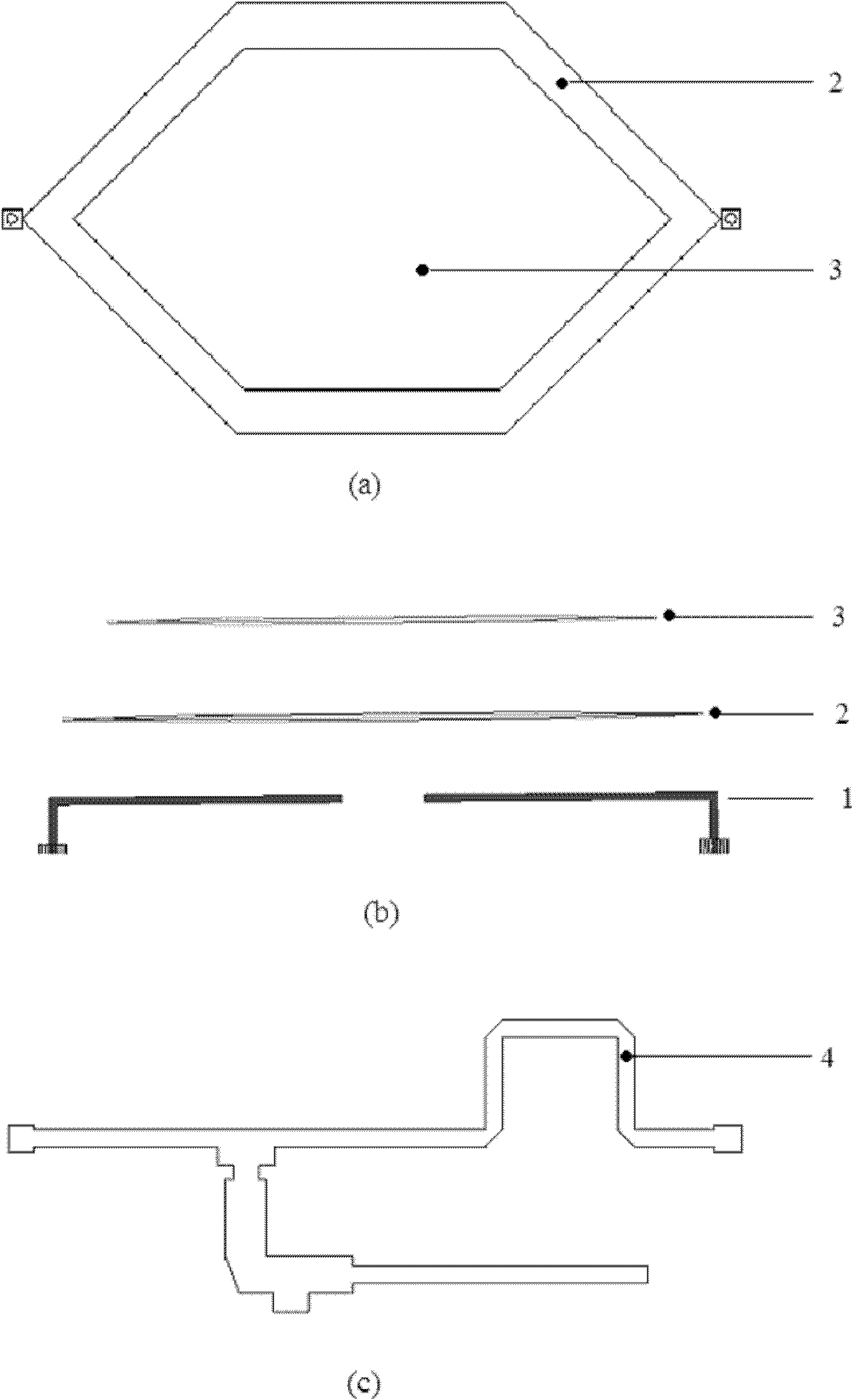
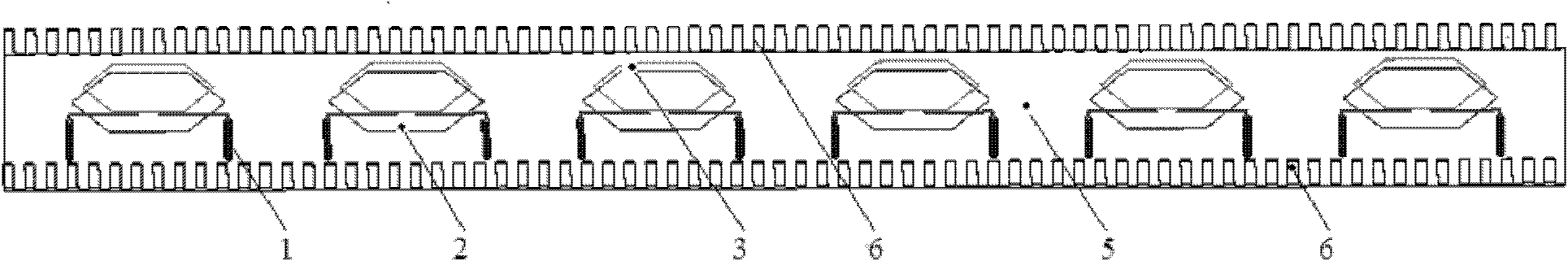
The invention discloses an array antenna of a wide-band and low-profile beam wireless communication base station, which comprises an array unit of the array antenna. The array antenna of the wide-band and low-profile beam wireless communication base station is characterized in that: an excited radiating patch and a parasitic radiating patch of the array unit are both in a shape in which the middle is rectangular and two ends are conical; an L-shaped excitation probe below the excited radiating patch performs equal-amplitude and reverse-phase coupling feed on the two ends of the excited radiating patch; and a metal gap folded edge is arranged on a longitudinal side edge of a reflecting plate. The array antenna of the wide-band and low-profile beam wireless communication base station has wide impedance characteristics and low profile, and can obtain a more accurate beam width within a wide working band.

Application Domain

Radiating elements structural formsIndividually energised antenna arrays

Technology Topic

Frequency bandPhysics +4

Image

  • Array antenna of wide-band and low-profile beam wireless communication base station
  • Array antenna of wide-band and low-profile beam wireless communication base station
  • Array antenna of wide-band and low-profile beam wireless communication base station

Examples

  • Experimental program(1)

Example Embodiment

The present invention and its advantages will be further explained below with reference to FIG. 1 and FIG. 2.
Referring to Figure 1, the array unit of the present array antenna is a radiation patch (including excitation radiation patch and parasitic radiation patch) fed by an L-shaped excitation probe. The middle of the radiation patch is rectangular, and both ends are tapered gradual structures. Under the excitation radiation patch, two L-shaped excitation probes are used to couple and feed the two ends of the excitation radiation patch. The L-shaped excitation probe is connected to the microstrip line feed network located on the ground plane. The sheet material of the microstrip line feeder network is a polytetrafluoroethylene sheet with a dielectric constant εr=2.65 and a thickness of 1mm. The two output ports of the microstrip feed network have the same signal amplitude but opposite phase. Using double L-shaped excitation probes with constant amplitude and reverse phase excitation methods can make the current distribution on the excitation radiation patch and the parasitic radiation patch more uniform, make the E-plane pattern more symmetrical, and further improve the antenna gain. On top of the exciting radiation patch, a parasitic radiation patch that is also tapered at both ends is added. Taking into account the characteristics of the beam width and front-to-back ratio of the azimuth plane pattern, the width, length and ground height of the excitation radiation patch are respectively designed as 0.243λ0, 0.496λ0 and 0.096λ0, and the width, length and ground height of the parasitic radiation patch They are respectively 0.198λ0, 0.425λ0 and 0.17λ0, and λ0 is the free space wavelength corresponding to the center frequency. The radiation patch used in the present invention is longer than the conventional radiation patch, so the gain of the radiation patch of the present invention is higher than that of the conventional radiation patch. Changing the two ends of the radiating patch into a tapered shape not only increases the antenna gain, but also facilitates impedance matching. The size of the parasitic radiation patch is relatively smaller than the size of the excitation radiation patch. The parasitic radiation patch not only has the function of impedance adjustment, but also has the function of improving the radiation pattern.
Compared with Figure 2, this antenna includes 6 array elements, each of which is excited in the same amplitude and phase. The array spacing is 0.82λ0. If the width of the reflector is designed to be 0.55λ0, and two metal folds with a height of 0.128λ0 are added to the periphery, the beam width of the azimuth plane is close to 78° in the entire frequency band, which is about less than the specification. The value in 90±8°, it is even impossible to achieve a more accurate beam width of 90±2°. At this time, if the width of the reflector is narrowed, the beam width can be widened to approach the beam width specified in the specification, but the standing wave ratio and front-to-back ratio of the array antenna will also change at this time, deviating from the specification. The direction of the prescribed value develops. In order to broaden the beam width while keeping other characteristics unchanged, the present invention adopts a reflector plate with gap metal flanges. The width of the metal fold of the slot is 0.031λ0, the slot pitch is 0.069λ0, and the slot height is 0.128λ0. The slot is equivalent to an additional radiator that is re-excited by the excitation radiation patch and the parasitic radiation patch. The electric field of the observation point in the far area is the vector superposition of the radiation field of the slit and the radiation field of the radiation patch. Because the input impedance of the radiation patch and the slot are different, the phase of the original electric field generated by the radiation patch and the slot is also different. At the same time, the distance between the observation point in the far area and the radiation patch and the slot is also different, resulting in the difference in distance. The phase difference is also different. In this way, the field of the observation point in the far area is determined by the shape of the array unit and the shape of the reflector (including the seam hemming). Under the condition that other characteristics have met the technical specifications, the beam width can be adjusted in a small range by changing the shape of the metal flange of the slot, so that it has a more accurate beam width, while other characteristics remain almost unchanged.
The standing wave ratio measured by the entire antenna (including the microstrip feeder network) is less than 1.5 in the entire frequency band. One antenna can simultaneously cover GSM1800 (1710~1880MHz), CDMA1900 (1850~1990MHz) and ITU'sIMT-2000 (1885~ 2170MHz) frequency band, simplifies the composition of the communication system, reduces the cost, and increases the reliability of the system. The measured radiation pattern is shown in Figure 3. It can be seen that the sidelobe level is less than -10dB, and the beam width of the azimuth plane is 92±2° in the entire frequency band, which is far better than the value 92±8° specified in the technical specifications of the wireless communication base station antenna. The front-to-back ratio level of the pattern is 25dB, which meets the technical specifications of wireless communication base station antennas. The net gain of the array antenna (after deducting the feeder loss) is 15.0dBi in the entire frequency band. The above test results show the effectiveness of the array antenna design.

PUM

no PUM

Description & Claims & Application Information

We can also present the details of the Description, Claims and Application information to help users get a comprehensive understanding of the technical details of the patent, such as background art, summary of invention, brief description of drawings, description of embodiments, and other original content. On the other hand, users can also determine the specific scope of protection of the technology through the list of claims; as well as understand the changes in the life cycle of the technology with the presentation of the patent timeline. Login to view more.

Similar technology patents

An improved drone structure

ActiveUS20160214728A1reduce weight
Owner:UNIVERSITY OF FLORENCE

Lightweight damper pulley

InactiveUS20120231909A1easily manufacturereduce weight
Owner:FUKOKU KOREA

Sealing structure for high-pressure container

InactiveUS20090071930A1increased pressure resistancereduce weight
Owner:YACHIYO IND CO LTD

Heat sink

ActiveUS20160324031A1reduce weightstrong bonding strength
Owner:JNC CORP

High isolation protection material and preparation method thereof

Owner:THE QUARTERMASTER EQUIPMENT RESEARCH INSTITUTE OF THE GENERAL LOGISITIC DEPARTME +1

Classification and recommendation of technical efficacy words

  • reduce weight

Electrically driven brake booster

InactiveUS20020158510A1reduce weightsimple construction
Owner:BOSCH AUTOMOTIVE SYST CORP

Display device

ActiveUS20140043546A1reduce weightreduce detection sensitivity
Owner:SEMICON ENERGY LAB CO LTD

Curved Automatic-Darkening Filter

InactiveUS20140168546A1reduce weightlow weight
Owner:3M INNOVATIVE PROPERTIES CO

Thermal Solution for Prismatic Lithium Ion Battery Pack

ActiveUS20130115506A1reduce weight
Owner:NEOGRAF SOLUTIONS LLC
Why Eureka
Try Eureka