Printed circuit board (PCB) and manufacturing method thereof

A printed circuit board and printed circuit technology, which is used in printed circuit manufacturing, printed circuits, printed circuit components, etc., can solve problems such as board warping, uneven energy distribution, and no heat absorption in the hollow area of ​​the printed circuit board.

Active Publication Date: 2011-06-29
PEKING UNIV FOUNDER GRP CO LTD +1
View PDF1 Cites 7 Cited by
  • Summary
  • Abstract
  • Description
  • Claims
  • Application Information

AI Technical Summary

Problems solved by technology

[0003] However, the existing technology has the following disadvantages: the hollow area of ​​the printed circuit board does not absorb heat energy, and the copper in the broken edge and the outer shape area absorbs a large amount of heat energy during the heating process, resulting in uneven energy distribution and board warpage
When performing SMT mounting, usually the circuit board manufactured by the PCB supplier is directly mounted without any processing. When the circuit board passes through the SMT high-temperature mounting, due to the high temperature, the circuit board is closed around the broken edge Under the circumstances, the copper foil will expand rapidly when heated, and the copper foil will be stretched in a certain direction under the action of thermal stress, causing the board to warp, resulting in defective parts.

Method used


Image

  • Printed circuit board (PCB) and manufacturing method thereof
  • Printed circuit board (PCB) and manufacturing method thereof
  • Printed circuit board (PCB) and manufacturing method thereof

Examples


Embodiment 1

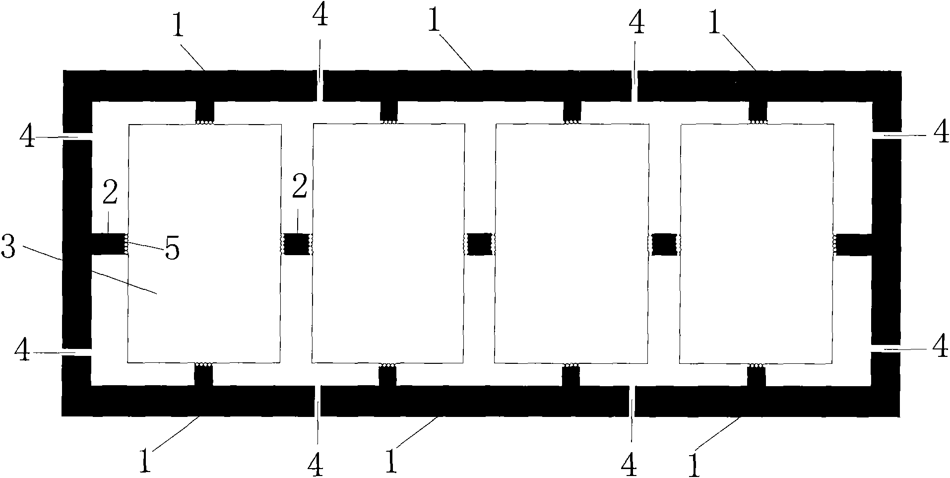
[0020] The printed circuit board shown in the first embodiment includes a printed circuit layer and an insulating layer. Such as figure 1 As shown, the printed circuit layer and the insulating layer both include a connecting piece 2, a breaking edge 1 and four exterior areas 3 located inside the breaking edge. Each shape area 3 is connected to the broken edge 1 through a connecting piece 2. A stamp hole 5 is provided on the connecting piece 2. The stamp hole is convenient for separating the shape area after the patch is pasted. The broken edge of the printed circuit layer is provided with a Eight openings 4.

[0021] Further, the width of the opening is 1.2-1.3mm, preferably 1.27mm.

[0022] Further, the distance between adjacent openings on the same side of the broken edge is 50-100 mm.

[0023] Further, the opening on the printed circuit layer may be symmetrical with respect to the central axis of the printed circuit layer or the opening may be symmetrical with respect to...

Embodiment 2

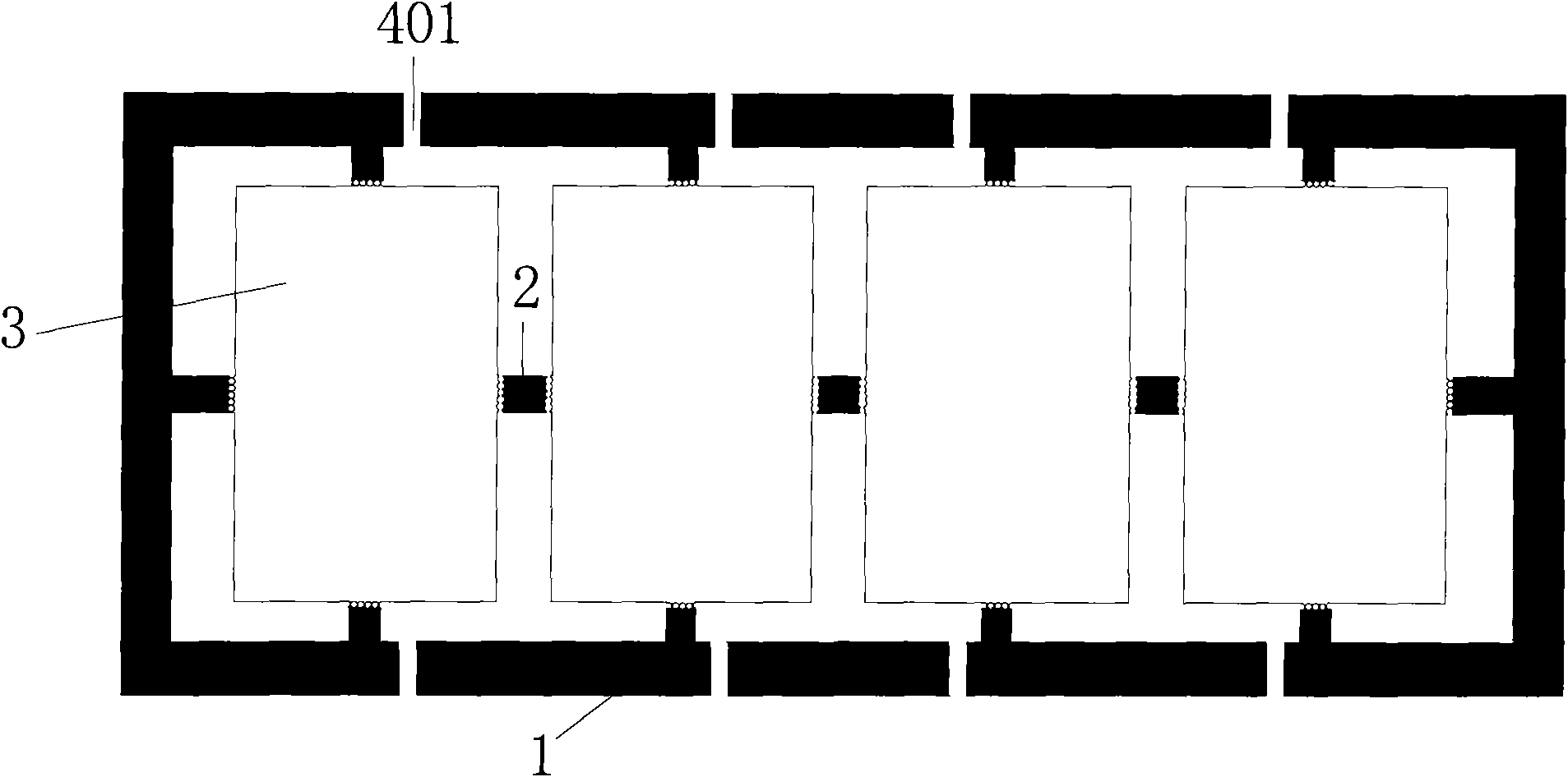
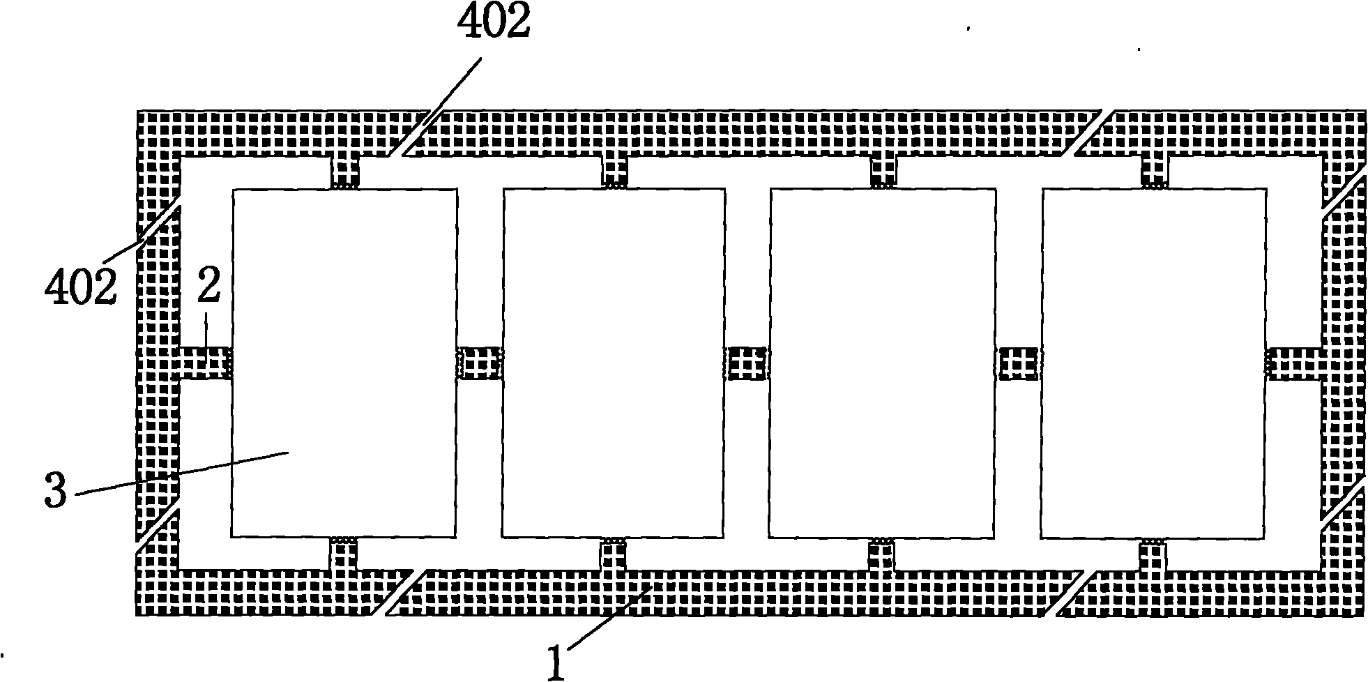
[0027] The printed circuit board shown in the second embodiment includes four layers of printed circuit layers and three layers of insulating layers, wherein each layer of printed circuit layers and insulating layers includes a connecting piece, a breaking edge and four exterior areas located inside the breaking edge , hollowed out between the broken edge and the shape area, and connected between each shape area and each shape area and the broken edge through a connecting piece, and eight openings are provided at the broken edge of each printed circuit layer.

[0028] Further, the width of the opening is 1.2-1.3mm, preferably 1.27mm.

[0029] Further, the distance between adjacent openings on the same side of the broken edge is 50-100mm.

[0030] Further, the openings on adjacent printed circuit layers are staggered up and down, and the staggered distance is 20-50 mm in the direction parallel to the printed circuit layer.

[0031] In this way, the uneven thickness of the edge...

Embodiment 3

[0040] Embodiment three manufacturing method flow chart such as Figure 4 As shown, including negative film production S101, negative film production includes:

[0041] Make a negative with a printed circuit pattern, and set an opening mark at the predetermined position of the broken edge of the printed circuit pattern. According to the size design of the plate, the distance between adjacent opening marks on the same side of the broken edge is 50-100mm, and printed on the same layer On the negative sheet of the circuit pattern, the opening is symmetrical to the central axis of the printed circuit pattern or symmetrical to the center of the printed circuit pattern; the width of the opening is 1.2-1.3 mm, and the optimal size is 1.27 mm.

[0042] If the circuit board includes multi-layer printed circuit layers, the direction of the opening mark at the predetermined position of the broken edge of the top layer and the bottom layer is perpendicular to the broken edge where the ope...


PUM


Abstract

The invention discloses a printed circuit board (PCB) and a manufacturing method thereof, and relates to the PCB and the manufacturing field thereof. The PCB is invented in order to eliminate the thermal stress effect of the circuit board. The PCB comprises at least one printed circuit layer and at least one insulating layer. Each printed circuit layer and each insulating layer comprise a connecting sheet, a broken edge and at least one profile area positioned inside the broken edge, wherein the part between the broken edge and the profile area is hollow; the profile areas, and the profile area and the broken edges are connected by the connecting sheets; and the broken edge of at least one printed circuit layer is provided with at least one opening. The invention further discloses a method for manufacturing the PCB. The invention is used for eliminating the thermal stress effect of the PCB while being adhered.

Description

technical field [0001] The invention relates to the field of printed circuit boards and the manufacture of printed circuit boards, in particular to a printed circuit board capable of eliminating the thermal stress effect of the printed circuit board itself and a manufacturing method thereof. Background technique [0002] As the precision of printed circuit boards is getting better and better, SMT manufacturers have gradually increased their requirements for the high temperature resistance performance of printed circuit boards and the overall quality of the board surface. At present, in the industry, in the production process of four-piece printed circuit boards, all the broken edges of the printed circuit board are covered with copper to form a closed whole. The appearance area of ​​the printed circuit board is connected to the broken edge. Integrity of the appearance of the board, hollow out between the broken edge and the appearance area of ​​each board, leaving a small co...

Claims


Application Information

Patent Timeline
Patent Type & Authority Applications(China)
IPC IPC(8): H05K1/02H05K3/00H05K3/06
Inventor 雷红慧代文艺
Owner PEKING UNIV FOUNDER GRP CO LTD
Why Eureka
Try Eureka