Printed circuit board (PCB) and manufacturing method thereof
A technology of printed circuit boards and printed circuits, which is applied in the direction of printed circuit manufacturing, printed circuits, printed circuit components, etc., and can solve problems such as uneven energy distribution, board warping, and hollow areas of printed circuit boards that do not absorb heat energy, etc.
- Summary
- Abstract
- Description
- Claims
- Application Information
AI Technical Summary
Problems solved by technology
Method used
Image
Examples
Embodiment 1
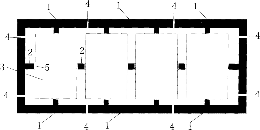
[0020] The printed circuit board shown in the first embodiment includes a printed circuit layer and an insulating layer. Such as figure 1 As shown, the printed circuit layer and the insulating layer both include a connecting piece 2, a breaking edge 1 and four exterior areas 3 located inside the breaking edge. Each shape area 3 is connected to the broken edge 1 through a connecting piece 2. A stamp hole 5 is provided on the connecting piece 2. The stamp hole is convenient for separating the shape area after the patch is pasted. The broken edge of the printed circuit layer is provided with a Eight openings 4.
[0021] Further, the width of the opening is 1.2-1.3mm, preferably 1.27mm.
[0022] Further, the distance between adjacent openings on the same side of the broken edge is 50-100 mm.
[0023] Further, the opening on the printed circuit layer may be symmetrical with respect to the central axis of the printed circuit layer or the opening may be symmetrical with respect to...
Embodiment 2
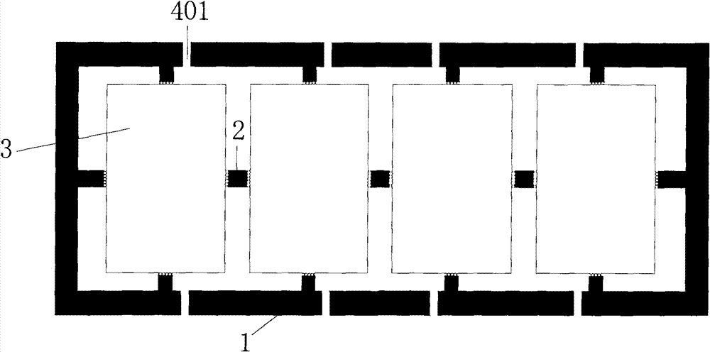
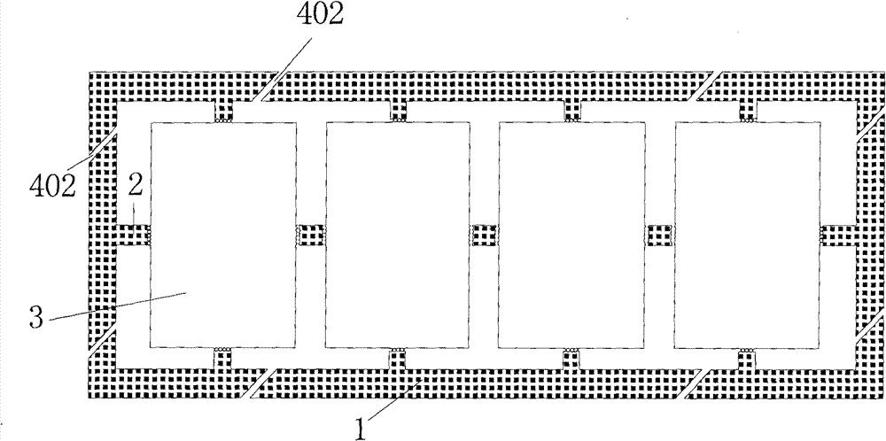
[0027] The printed circuit board shown in the second embodiment includes four layers of printed circuit layers and three layers of insulating layers, wherein each layer of printed circuit layers and insulating layers includes a connecting piece, a breaking edge and four exterior areas located inside the breaking edge , hollowed out between the broken edge and the shape area, and connected between each shape area and each shape area and the broken edge through a connecting piece, and eight openings are provided at the broken edge of each printed circuit layer.
[0028] Further, the width of the opening is 1.2-1.3mm, preferably 1.27mm.
[0029] Further, the distance between adjacent openings on the same side of the broken edge is 50-100mm.
[0030] Further, the openings on adjacent printed circuit layers are staggered up and down, and the staggered distance is 20-50 mm in the direction parallel to the printed circuit layer.
[0031] In this way, the uneven thickness of the edge...
Embodiment 3
[0040] Embodiment three manufacturing method flow chart such as Figure 4 As shown, including negative film production S101, negative film production includes:
[0041] Make a negative with a printed circuit pattern, and set an opening mark at the predetermined position of the broken edge of the printed circuit pattern. According to the size design of the plate, the distance between adjacent opening marks on the same side of the broken edge is 50-100mm, and printed on the same layer On the negative sheet of the circuit pattern, the opening is symmetrical to the central axis of the printed circuit pattern or symmetrical to the center of the printed circuit pattern; the width of the opening is 1.2-1.3 mm, and the optimal size is 1.27 mm.
[0042] If the circuit board includes multi-layer printed circuit layers, the direction of the opening mark at the predetermined position of the broken edge of the top layer and the bottom layer is perpendicular to the broken edge where the ope...
PUM
 Abstract
Description
Claims
Application Information


