Chip provided with high electrostatic discharge performance

An electrostatic discharge and chip technology, applied in circuits, electrical components, electrical solid devices, etc., can solve the problems of reducing the normal working performance of the analog domain and the digital domain to the analog domain, and achieve the effect of improving the ESD protection performance.

Inactive Publication Date: 2011-07-06
WUXI ZGMICRO ELECTRONICS CO LTD
View PDF5 Cites 1 Cited by
  • Summary
  • Abstract
  • Description
  • Claims
  • Application Information

AI Technical Summary

Problems solved by technology

[0014] However, since the ground pin 212 is connected to the electrostatic discharge ground wire ESDVSS1, the noise jitter in the digital domain will be transferred to the analog domain, thereby reducing the normal working performance of the analog domain, such as the signal-to-noise ratio and other indicators

Method used


Image

  • Chip provided with high electrostatic discharge performance
  • Chip provided with high electrostatic discharge performance
  • Chip provided with high electrostatic discharge performance

Examples


Embodiment Construction

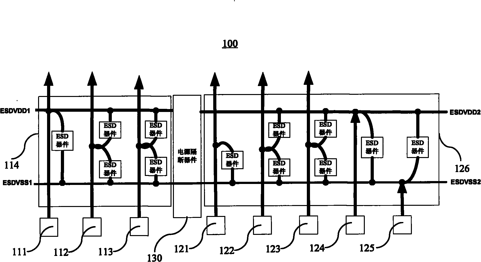
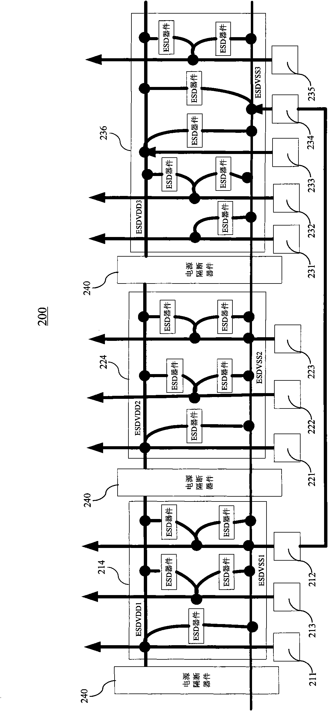
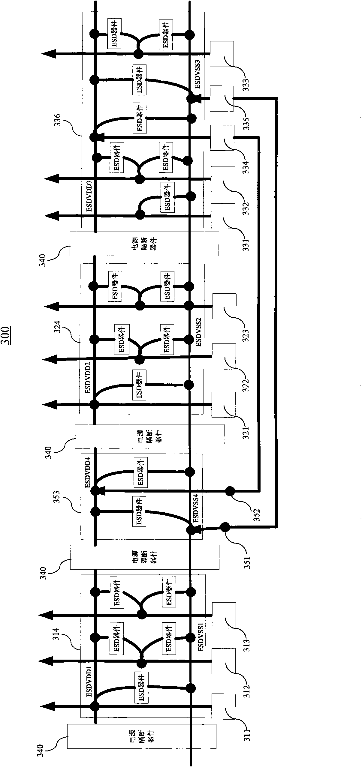
[0029] The detailed description of the present invention directly or indirectly simulates the operation of the technical solution of the present invention mainly through programs, steps, logic blocks, processes or other symbolic descriptions. In the ensuing description, numerous specific details are set forth in order to provide a thorough understanding of the present invention. Rather, the invention may be practiced without these specific details. These descriptions and representations herein are used by those skilled in the art to effectively convey the substance of their work to others skilled in the art. In other words, for the purpose of avoiding obscuring the present invention, well-known methods, procedures, components and circuits have not been described in detail since they are readily understood.

[0030] Reference herein to "one embodiment" or "an embodiment" refers to a particular feature, structure or characteristic that can be included in at least one implementa...


PUM


Abstract

The invention provides a chip provided with a high electrostatic discharge performance, which comprises a numerical field and a plurality of simulation fields, wherein the numerical field comprises a grounding pin, a power pin, a signal pin and an electrostatic protection circuit; each simulation circuit comprises a grounding pin, a power pin, a signal pin and an electrostatic protection circuit; the electrostatic protection circuit in the numerical field comprises an electrostatic discharge power wire connected with the power pin, and an electrostatic discharge ground wire connected with the grounding pin in the field; and the electrostatic protection circuit in each numerical field comprises an electrostatic discharge ground wire and an electrostatic discharge power wire connected with power pin in the field. Electrostatic discharge ground wires in two adjacent fields are connected together, an electrostatic discharge grounding terminal is led out of each electrostatic discharge ground wire, and the electrostatic discharge grounding terminals are connected with the grounding pin in the numerical field through wires. Therefore, a passage with higher electrostatic discharge capacity is additionally established.

Description

【Technical field】 [0001] The invention relates to the field of ESD design, in particular to a chip with high ESD performance. 【Background technique】 [0002] ESD (Electro-Static discharge) means "electrostatic discharge". Static electricity is an objective natural phenomenon, which is unevenly distributed on the chip itself, on the human body and on the machine, as well as the environment where the chip can exist and the surrounding things. These static charges may be released in some way at any time. The characteristics of electrostatic discharge are high voltage, low power, small current and short action time. It is very important to improve the protection ability of an integrated circuit (IC, also called a chip) to electrostatic discharge. [0003] The purpose of electrostatic protection in the chip is to prevent the working circuit of the chip from being damaged by the electrostatic discharge path, and to ensure that there is a suitable electrostatic discharge path fo...

Claims


Application Information

Patent Timeline
Patent Type & Authority Applications(China)
IPC IPC(8): H01L27/02H01L23/60
Inventor 刘子熹
Owner WUXI ZGMICRO ELECTRONICS CO LTD
Why Eureka
Try Eureka