ESD protection structure

a protection structure and parasitic silicon technology, applied in the direction of semiconductor devices, semiconductor/solid-state device details, electrical apparatus, etc., can solve the problems of unstable electrostatic trigger voltage, difficult to solve, damage to electronic products, etc., to improve the voltage breakdown position, improve the esd protection performance, and improve the esd turning-on performance of a parasitic silicon controlled rectifier.

Active Publication Date: 2012-03-29
SHANGHAI HUAHONG GRACE SEMICON MFG CORP
View PDF7 Cites 13 Cited by
  • Summary
  • Abstract
  • Description
  • Claims
  • Application Information

AI Technical Summary

Benefits of technology

[0035]The device used as an ESD protection structure of the present invention can improve the ESD turning-on performance of a parasitic silicon controlled rectifier without affecting the driving function of the device and can further improve the ESD protection performance. Specifically, it can improve the voltage breakdown position when ESD occurs and further improve the device stability in ESD protection. The present invention can also adjust electrostatic trigger voltage through parameters setting, rapidly turn on a vertical parasitic transistor, and reduce the damage of voltage breakdown to the channel region of the device and hence the risk of failure to turn-on the vertical parasitic transistor.

Problems solved by technology

Electrostatic discharge (ESD) may cause damage to electronic products and it is difficult to be solved.
However, this adjustment may lead to an unstable avalanche breakdown voltage and therefore forms an unstable electrostatic trigger voltage therefrom.

Method used


Image

  • ESD protection structure
  • ESD protection structure
  • ESD protection structure

Examples


Embodiment Construction

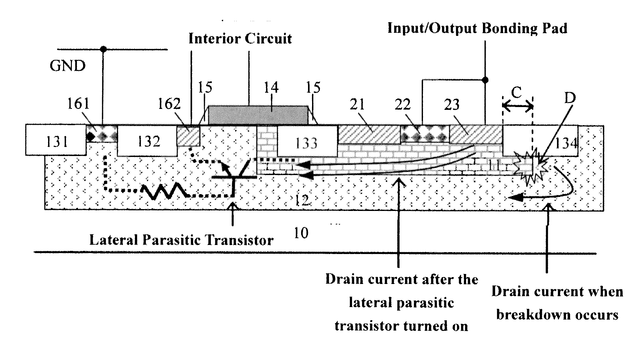
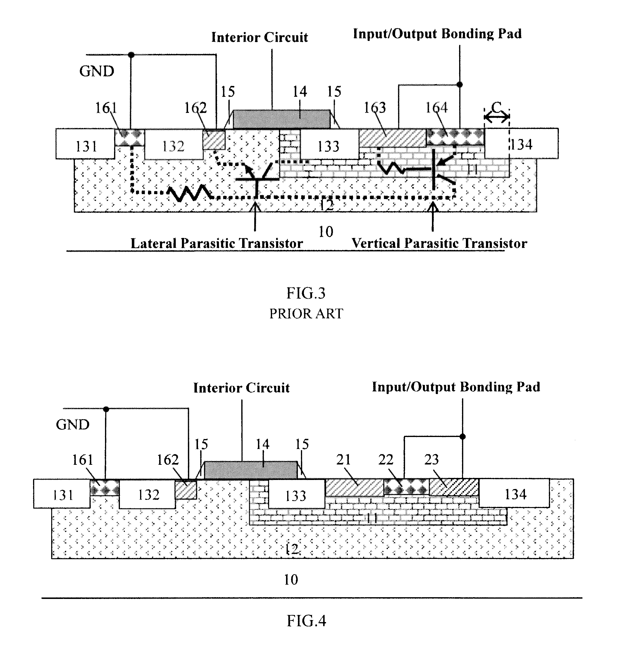
[0044]As shown in FIG. 4, the device of the present invention used as an ESD protection structure is also an N-type LDMOS device. The device includes a P-type substrate 10, a P-type well 12 in the P-type substrate 10, and a N-type lightly doped region 11 in the P-type well 12. Isolation structures 131, 132 are formed in the P-type well 12, an isolation structure 133 is formed in the N-type lightly doped region 11, and an isolation structure 134 is formed in the N-type lightly doped region 11 and / or the P-type well 12, wherein the isolation structures 131, 132, 133, and 134 are structures such as LOCOS (Local Oxidation of Silicon) structures or STI (Shallow Trench Isolation) structures. A gate 14 is formed on the P-type well 12, wherein one side of the gate is on the P-type well 12 and the other side is on the isolation structure 133, and spacers 15 are formed on both sides of the gate 14. Wherein, the material of the gate 14 is such as polysilicon, and the material of the spacers 15...


PUM


Abstract

A device used as an ESD protection structure, which is a modified N-type LDMOS device is disclosed. A conventional LDMOS includes only one N-type heavily doped region as a drain in an N-type lightly doped region (11), while the device of the invention includes a P-type heavily doped region (22) in an N-type lightly doped region (11), dividing the N-type heavily doped region into two N-type heavily doped regions (21, 23) unconnected and independent to each other. The N-type heavily doped region (21) close to the gate (14) has no picking-up terminal. The N-type heavily doped region (23) away from the gate (14) together with the P-type heavily doped region (22) is picked up and connected to an input/output bonding pad.

Description

CROSS-REFERENCES TO RELATED APPLICATIONS[0001]This application claims the priority of Chinese patent application number 201010290452.X, filed on Sep. 25, 2010, the entire contents of which are incorporated herein by reference.FIELD OF THE INVENTION[0002]The present invention relates to a semiconductor integrated circuit device and, more particularly, to a MOS transistor used as an ESD protection structure of a high-voltage circuit.BACKGROUND[0003]Electrostatic discharge (ESD) may cause damage to electronic products and it is difficult to be solved. At present, the most commonly used ESD protection structure for semiconductor integrated circuits is GGMOS (Ground Gate MOSFET). A GGMOS device includes a low-voltage MOS (namely ordinary MOS transistor), an LDMOS (Lateral Diffusion MOSFET) and a DDDMOS (Double Diffusion Drain MOSFET), etc. Wherein, the low-voltage MOS is mainly used as an ESD protection structure for low-voltage circuits, while the LDMOS and DDDMOS are used as ESD protec...

Claims


Application Information

Patent Timeline
Patent Type & Authority Applications(United States)
IPC IPC(8): H01L29/772
CPCH01L27/027H01L29/0649H01L29/0834H01L29/7835H01L29/7436H01L29/749H01L29/1016
Inventor GAO, XIANG
Owner SHANGHAI HUAHONG GRACE SEMICON MFG CORP
Why Eureka
Try Eureka