Electrostatic discharge protection device and manufacturing method thereof

a protection device and electrostatic discharge technology, applied in semiconductor devices, diodes, electrical equipment, etc., can solve the problems of increasing the vulnerability of the external environment, increasing the risk of electrostatic discharge (esd) to modern electronics, and destroying unprotected ics, etc., to achieve the effect of improving the performance of the esd protection devi

Active Publication Date: 2018-09-04
UNITED MICROELECTRONICS CORP
View PDF3 Cites 0 Cited by
  • Summary
  • Abstract
  • Description
  • Claims
  • Application Information

AI Technical Summary

Benefits of technology

[0003]It is one of the objectives of the present invention to provide an electrostatic discharge (ESD) protection device and a manufacturing method thereof. In the ESD protection device and the manufacturing method thereof in the present invention, doped regions are formed in a metal oxide semiconductor (MOS) structure for forming silicon control rectifier (SCR) configurations embedded in the MOS structure and the performance of the ESD protection device may be improved accordingly.

Problems solved by technology

As products based on ICs become more delicate, they also become more vulnerable to the impacts of the external environment.
For example, it is found that electrostatic discharge (ESD) is a constant threat to modern electronics.
The result of ESD on unprotected ICs is often destruction, characterized by melting or explosion of apart of the ICs.

Method used


Image

  • Electrostatic discharge protection device and manufacturing method thereof
  • Electrostatic discharge protection device and manufacturing method thereof
  • Electrostatic discharge protection device and manufacturing method thereof

Examples


Embodiment Construction

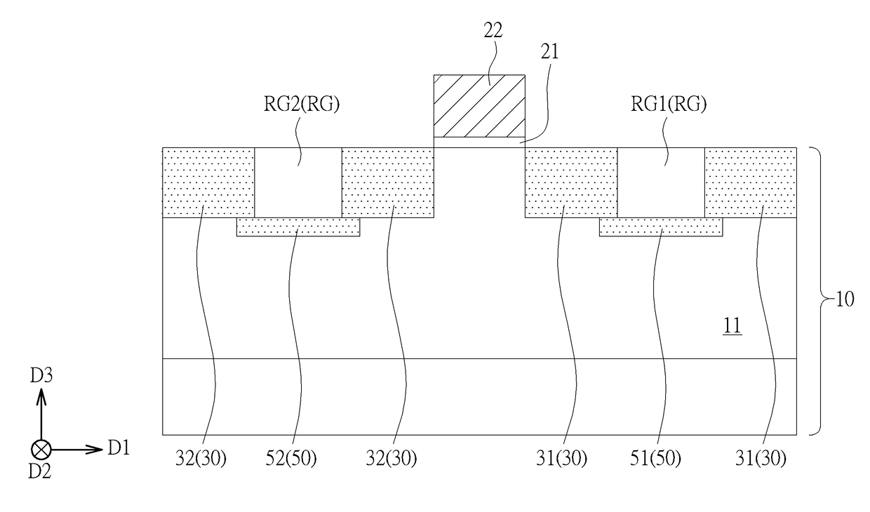
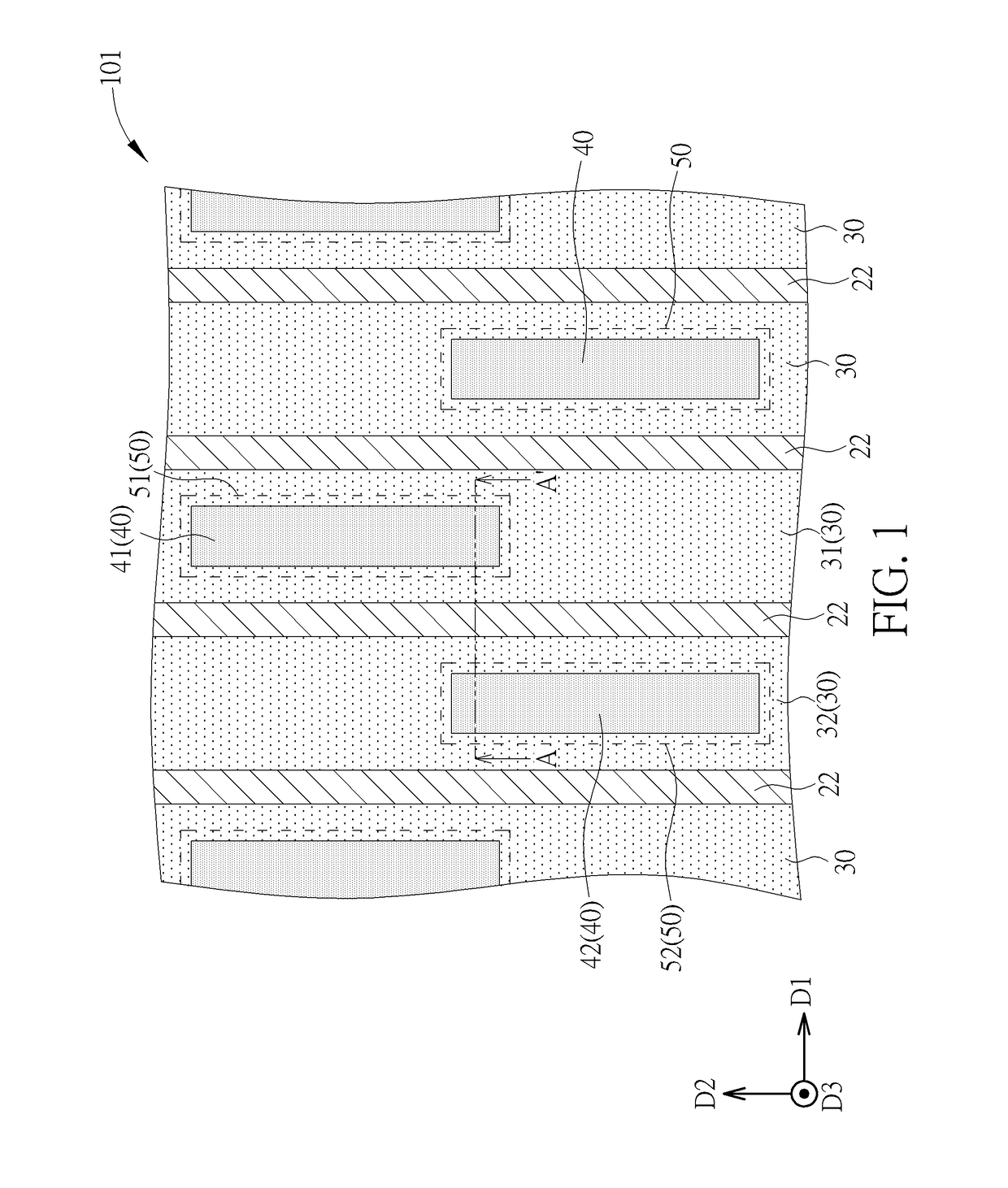
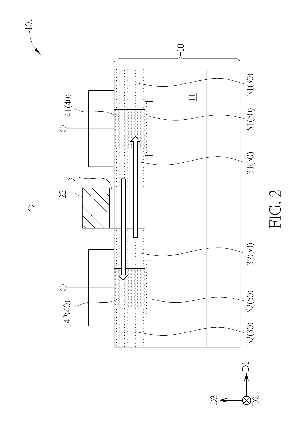
[0017]Please refer to FIG. 1 and FIG. 2. FIG. 1 is a schematic top view diagram illustrating an electrostatic discharge (ESD) protection device according to a first embodiment of the present invention. FIG. 2 is a cross-sectional drawing taken along a line A-A′ in FIG. 1. As shown in FIG. 1 and FIG. 2, an ESD protection device 101 is provided. The ESD protection device 101 includes a semiconductor substrate 10, a well 11, at least one gate structure 22, a first source / drain region 31, a second source / drain region 32, a first doped region 41, and a second doped region 42. The semiconductor substrate 10 in this embodiment may include a silicon substrate, an epitaxial silicon substrate, a silicon germanium substrate, a silicon carbide substrate, or a silicon-on-insulator (SOI) substrate, but not limited thereto. The well 11 is disposed in the semiconductor substrate 10. The well may include an N-type well or a P-type well. The gate structure 22 is disposed on the semiconductor substrat...


PUM


Abstract

An ESD protection device includes a semiconductor substrate, a well, a gate structure, a first source/drain region, a second source/drain region, a first doped region, and a second doped region. The well is disposed in the semiconductor substrate. The gate structure is disposed on the well. The first source/drain region and the second source/drain region are disposed in the well and disposed at two opposite sides of the gate structure respectively. The first doped region is disposed in the first source/drain region. The second doped region is disposed in the second source/drain region. A conductivity type of the first doped region is complementary to that of the first source/drain region. A conductivity type of the second doped region is complementary to that of the second source/drain region. A conductivity type of the well is complementary to that of the first source/drain region and the second source/drain region.

Description

BACKGROUND OF THE INVENTION1. Field of the Invention[0001]The present invention relates to an electrostatic discharge (ESD) protection device and a manufacturing method thereof, and more particularly, to an ESD protection device having a MOS structure and a manufacturing method thereof.2. Description of the Prior Art[0002]Chips and / or integrated circuits (ICs) are the most essential hardware foundation of the modern information field. As products based on ICs become more delicate, they also become more vulnerable to the impacts of the external environment. For example, it is found that electrostatic discharge (ESD) is a constant threat to modern electronics. The result of ESD on unprotected ICs is often destruction, characterized by melting or explosion of apart of the ICs. Therefore, the ESD protection devices are regarded as important components of the protection circuitry provided in electronic devices. Typically, during a normal IC operation, the ESD protection device is turned ...

Claims


Application Information

Patent Timeline
Patent Type & Authority Patents(United States)
IPC IPC(8): H01L29/06H01L29/66H01L29/08H01L29/749H01L29/10H01L27/02
CPCH01L27/027H01L29/1095H01L29/0847H01L29/0653H01L29/749H01L29/66356H01L27/0262H01L29/0692H01L29/1083H01L29/7436H01L29/78
Inventor YEN, SHIH-CHELAI, PO-YATANG, TIEN-HAOSU, KUAN-CHENG
Owner UNITED MICROELECTRONICS CORP
Why Eureka
Try Eureka