ESD protection circuit

a protection circuit and electrostatic discharge technology, applied in semiconductor devices, semiconductor/solid-state device details, electrical apparatus, etc., can solve the problems of increasing the size of the transistor, the transistor cannot discharge as large an esd pulse, and the inability to trigger the parasitic transistor, so as to improve the uniformity of turn-on, improve the performance of the esd protection structure, and reduce the size of the protection structure.

Active Publication Date: 2012-07-10
ALTERA CORP
View PDF2 Cites 16 Cited by
  • Summary
  • Abstract
  • Description
  • Claims
  • Application Information

AI Technical Summary

Benefits of technology

[0008]In an illustrative embodiment of the invention, elongated floating wells are located on opposite sides of the gate structure between two of the substrate taps and the ends of the gates. Thus, the floating wells extend in a direction substantially perpendicular to the direction in which the gate fingers extend. As a result, the floating wells effectively isolate these two substrate taps and force current flow in the substrate under the multifingered gate transistor to be substantially perpendicular to the direction in which the gate fingers extend. This increases the potential difference between these substrate regions and adjacent source regions in the multi-fingered gate transistor, thereby aiding the triggering of the parasitic bipolar transistors under adjacent gate fingers into a high current state. This also reduces the differences among the potentials in the substrate under the different source regions and thus improves the uniformity of turn-on of the parasitic bipolar transistors under the gate fingers. Because the floating wells effectively isolate two of the substrate taps, it is not necessary to maintain as great a distance from them as in prior art devices. Moreover, because the floating wells significantly improve the performance of the ESD protection structure, some of this performance improvement may be exchanged for decreases in the size of the protection structure.

Problems solved by technology

Since the triggering of the parasitic bipolar transistor depends on forward biasing the P-N junction between the P-type substrate and the N-type source region, the potential difference at some portions of the multi-fingered structure between the substrate and the adjacent source regions may not be enough to trigger the parasitic transistor in those portions.
Thus, triggering of the transistor tends to be non-uniform with the result that the transistor is not able to discharge as large an ESD pulse as it could if triggering were substantially uniform across the entire multi-fingered structure.
The penalty for this, however, is that there is a substantial gap 235 between the gate fingers and the P-type substrate tap resulting in an increase in the size of the transistor.

Method used


Image

  • ESD protection circuit
  • ESD protection circuit
  • ESD protection circuit

Examples


Embodiment Construction

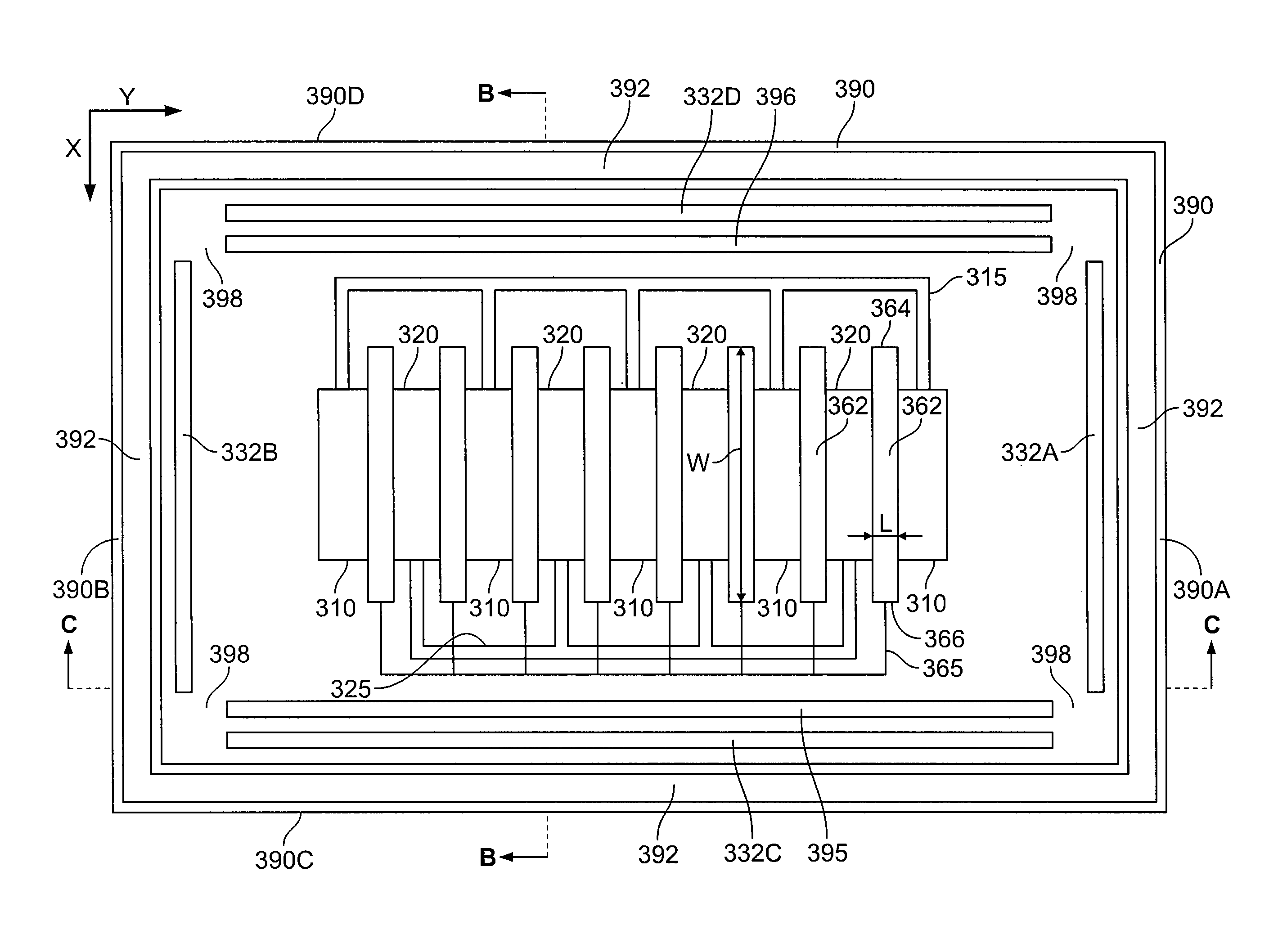
[0016]In accordance with one aspect of the invention, we have modified the structure of a multi-fingered MOS transistor so as to insert a floating well between the substrate tap and the gate fingers. FIGS. 3A, 3B and 3C depict a top view and two cross-sectional views of a multi-fingered gate structure 300 formed in accordance with this aspect of the invention. The cross-section of FIG. 3B is taken along the right-hand side of line B-B of FIG. 3A; and the cross-section of FIG. 3C is taken along the right-hand side of line C-C of FIG. 3A Structure 300 comprises N-type source and drain regions 310, 320 in a first P-type substrate 330 above a deep N-type well 340, an insulating layer (not shown) on the substrate and a multi-fingered gate 360 on the insulating layer. As shown in FIG. 3A, gate fingers 362 are parallel to one another, extend in a first direction X, and have first and second ends 364, 366. LDD regions (not shown) extend part way under each gate finger. As shown schematicall...


PUM


Abstract

A multi-fingered gate transistor is disclosed that is formed in a substrate of one conductivity type overlying a well of a second conductivity type. Ohmic contact to the well is made by an implanted region of the second conductivity type that circumscribes the multi-fingered gate transistor. Ohmic contact to the substrate is made by four taps located on four sides of the multi-fingered gate structure between the gate structure and the well contact. Floating wells are located on opposite sides of the gate structure between two of the substrate taps and the ends of the gates to isolate these substrate taps and force current flow in the substrate under the multifingered gate transistor to be substantially perpendicular to the direction in which the gate fingers extend. This increases the potential difference between these substrate regions and adjacent source regions in the multi-fingered gate transistor, thereby aiding the triggering of the parasitic bipolar transistors under adjacent gate fingers into a high current state. This also reduces the differences among the potentials in the substrate under the different source regions and thus improves the uniformity of turn-on of the parasitic bipolar transistors. As a result, it is not necessary to maintain as great a distance from the isolated substrate taps as in prior art devices. Moreover, because the floating wells significantly improve the performance of the ESD protection structure, some of this performance improvement may be exchanged for decreases in the size of the protection structure.

Description

BACKGROUND OF THE INVENTION[0001]This relates to electrostatic discharge (ESD) protection devices for protecting an integrated circuit from ESD damage.BACKGROUND OF THE INVENTION[0002]N-type metal-oxide-silicon (NMOS) transistors such as transistor 100 of FIG. 1 are a frequent choice for ESD protection circuits for integrated circuits. Transistor 100 comprises N-type source and drain regions 110, 120 in a P-type well 130 in substrate 140, an insulating layer 150 on the substrate and a gate 160 on the insulating layer between the source and drain regions. Sidewall spacers 162 are located on each side of gate 160; and lightly doped drain (LDD) regions 170, 180 extend part way under the gate from the source and drain regions. Transistor 100 operates to provide ESD protection by triggering a parasitic lateral bipolar transistor 190 inherent in the MOS structure where the source and drain regions 110, 120 of the MOS transistor constitute the emitter and collector of the lateral bipolar t...

Claims


Application Information

Patent Timeline
Patent Type & Authority Patents(United States)
IPC IPC(8): H01L23/62
CPCH01L23/62H01L2924/0002H01L2924/00
Inventor CHU, CHARLES Y.WATT, JEFFREY T.
Owner ALTERA CORP
Why Eureka
Try Eureka