Method for processing surface structure of aluminium substrate
A surface structure and treatment method technology, applied in the direction of surface reaction electrolytic coating, anodic oxidation, electrolytic coating, etc., to achieve the effect of promoting tight bonding, increasing bonding force, and improving high-voltage resistance
- Summary
- Abstract
- Description
- Claims
- Application Information
AI Technical Summary
Problems solved by technology
Method used
Image


Examples
Embodiment Construction
[0018] Below in conjunction with accompanying drawing and by embodiment the present invention will be described in further detail:
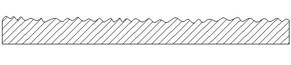
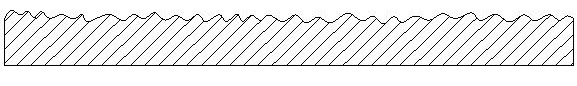
[0019] The method for treating the surface structure of the aluminum substrate provided by the present invention is a nano-processing method, mainly forming a rough and uniform honeycomb shape on the aluminum surface by pulse electroplating.
[0020] The method for treating the surface structure of the aluminum substrate of the present invention specifically includes the following steps:
[0021] S100. Pretreatment: Soak the aluminum substrate in NaOH solution with a water concentration of 10% for 10 minutes, and control the temperature at 40-45°C;
[0022] S200. Pulse electroplating: Use sulfuric acid, phosphoric acid, and oxalic acid to prepare the reaction solution in proportion, and then put the pretreated aluminum substrate into the reaction solution for pulse electroplating. The temperature is controlled between 13-24°C and the current dens...
PUM
 Abstract
Description
Claims
Application Information
PatSnap Eureka turns technology decisions into work you can execute. Powered by our Innovation Knowledge Graph, it runs expert workflows across engineering, life sciences, materials and intellectual property. Get your review-ready output in minutes.


