Light emitting diode array structure and manufacturing method thereof
A technology of light-emitting diodes and array structures, which is applied to electrical components, electrical solid-state devices, circuits, etc., and can solve problems such as difficult processes and damage to electrical connection structures
- Summary
- Abstract
- Description
- Claims
- Application Information
AI Technical Summary
Problems solved by technology
Method used
Image

Examples
Embodiment Construction
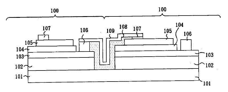
[0032] The invention discloses a light emitting diode array structure and a manufacturing method thereof. In order to make the description of the present invention more detailed and complete, please refer to the following description and cooperate with Figures 2A to 4 's icon.
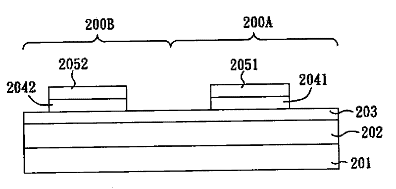
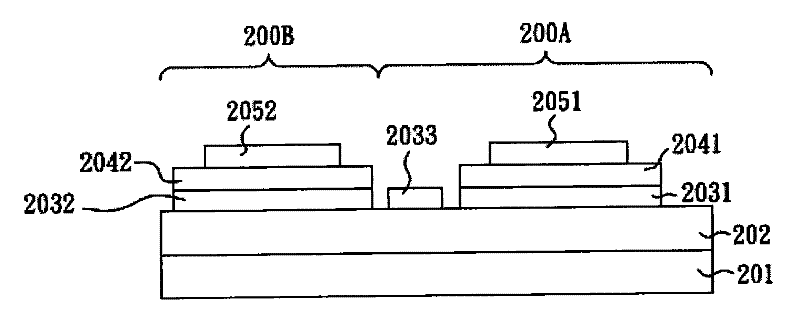
[0033] Figures 2A to 2K It is a schematic structural diagram of the manufacturing process according to the first embodiment of the present invention. like Figure 2A As shown, it includes a temporary substrate 201, a plurality of first light-emitting stacks 200A and a plurality of second light-emitting stacks 200B, wherein the plurality of first light-emitting stacks 200A and the plurality of second light-emitting stacks 200B are sequentially formed in the temporary on the substrate 201 . The first light emitting stack 200A includes an n-type semiconductor layer 203 formed on the temporary substrate 201, a first active layer 2041 formed on the n-type semiconductor layer 203, and a first p-type se...
PUM
 Abstract
Description
Claims
Application Information
 - R&D
- Intellectual Property
- Life Sciences
- Materials
- Tech Scout
- Unparalleled Data Quality
- Higher Quality Content
- 60% Fewer Hallucinations
Browse by: Latest US Patents, China's latest patents, Technical Efficacy Thesaurus, Application Domain, Technology Topic, Popular Technical Reports.
© 2025 PatSnap. All rights reserved.Legal|Privacy policy|Modern Slavery Act Transparency Statement|Sitemap|About US| Contact US: help@patsnap.com