
Welding column welding method for integrated circuit package

A technology of integrated circuits and welding methods, which is applied in the direction of circuits, welding equipment, electrical components, etc., can solve problems such as crack expansion of welding layers, open circuits, and the impact of device interconnection quality, and achieve the effect of improving yield and quality

Active Publication Date: 2011-07-27
WUXI ZHONGWEI GAOKE ELECTRONICS +1
View PDF2 Cites 12 Cited by
  • Summary
  • Abstract
  • Description
  • Claims
  • Application Information

AI Technical Summary

Problems solved by technology

The above-mentioned assembly method often has micro-encapsulated air bubbles on the welding surface, which affects the strength of the soldering column welding of packaged products, and the temperature change is likely to cause cracks in the soldering layer to expand, which will affect the quality of device interconnection and even lead to open circuits.

Method used


Image

  • Welding column welding method for integrated circuit package
  • Welding column welding method for integrated circuit package
  • Welding column welding method for integrated circuit package

Examples


Embodiment 1

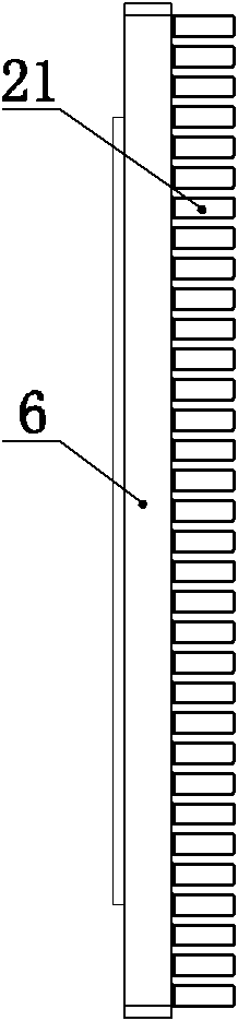
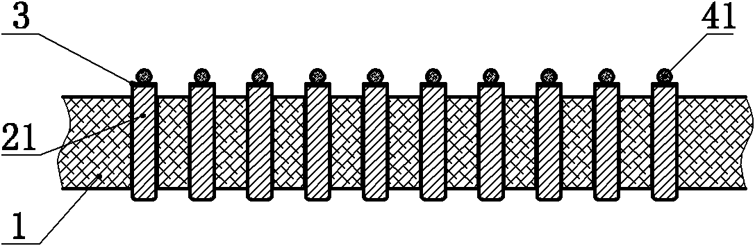
[0037] Such as figure 1 , figure 2 As shown, a CCGA560 packaged product with a pitch of 1.27 mm is assembled with Sn10Pb90 high-temperature solder pillars 21 with a diameter of φ0.89 mm. The post welding method of this product includes the following steps:

[0038] (1) Neatly arrange the Sn10Pb90 high-temperature solder columns 21 with a diameter of φ0.89mm in the special mold 1;

[0039] (2) Use a template to print flux 3 on the top of the high-temperature solder column 21, the brand of flux 3: WS-366 of INDIUM, etc.;

[0040] (3) According to the diameter of the high-temperature solder column 21, select the first solder ball 41 with a diameter of φ0.40 mm, and place the first solder ball 41 on the flux 3 on the top of the high-temperature solder column 21 with a ball-dropping template, see image 3 ;

[0041] (4) Put the mold 1 together with the high-temperature solder column 21, the flux 3 and the first solder ball 41 into the reflow furnace (at room temperature). The ...

Embodiment 2

[0048] Such as Figure 7 , Figure 8 As shown, a CCGA1144 packaged product with a pitch of 1.00 mm is assembled with an oxygen-free copper metal pillar 22 with a diameter of φ0.50 mm. The post welding method of this product includes the following steps:

[0049] (1) Neatly arrange the oxygen-free copper metal columns 22 with a diameter of φ0.50mm in the special mold 1;

[0050] (2) According to the diameter of the metal pillar 22, select the second solder ball 42 with a diameter of φ0.40mm with flux, and place the second solder ball 42 on the top of the metal pillar 22 with a ball placement device, see Figure 9 ;

[0051] (3) Put the mold 1 together with the metal pillar 22 and the second solder ball 42 into the heating table. The temperature-time process curve is determined by the second solder ball 42. The second solder ball 42 is melted by the heating table and then cooled to 60 Below ℃, the second solder ball 42 forms a half-moon spherical cap on the top of each metal...


PUM

PropertyMeasurementUnit
diameteraaaaaaaaaa

Abstract

The invention relates to a welding column welding method for integrated circuit package. The improvement is that: before a welding column is welded on a substrate, an outward-convex welding flux is formed at the top end of the welding column; and due to the point contact, surface tension of welding flux melting and other factors of the outward-convex welding flux, microbubbles do not exist during the fusing of the welding flux and the end surface so as to obtain a high-quality welding column package device without microbubbles on the welding surface. Through the invention, the problem that micro packing bubbles often exist on the welding surface of the welding column is solved without changing the existing welding equipment; the step of performing X ray or ultrasonic check on the device to ensure the welding quality of the conventional welding process is saved; and the welding quality is improved, and the welding yield is increased.

Description

technical field [0001] The invention relates to a soldering process for integrated circuit packaging pins, in particular to a soldering post welding method for integrated circuit packaging, which belongs to the technical field of integrated circuit manufacturing. Background technique [0002] With the increase in the number of I / O terminals of semiconductor integrated circuit devices and the increase in packaging density, the packaging terminals are arranged in area arrays, such as ball grid arrays (BGA) and column grid arrays (CGA), and the pitch is getting more and more The smaller (2.54mm→1.27mm→1.00mm→0.80mm→...). [0003] The process method of using welding pillars to assemble and weld the required column grid array (CGA) package mainly uses printing solder paste such as silk screen or stainless steel plate or distributes solder paste with precision dispensing process, and then puts the welding pillars into the mold or puts them into the mold. After the overall welding...

Claims


Application Information

Patent Timeline
Patent Type & Authority Applications(China)
IPC IPC(8): H01L21/60B23K1/008
Inventor 丁荣峥杨兵张顺亮
Owner WUXI ZHONGWEI GAOKE ELECTRONICS
Learn More