Welding method for welding columns of encapsulated integrated circuit (IC)

A welding method and integrated circuit technology, applied in the direction of circuits, welding equipment, electrical components, etc., can solve problems such as crack expansion in the welding layer, open circuits, and affecting the welding strength of soldering pillars of packaged products, so as to improve the yield and quality of products. Effect

Active Publication Date: 2011-08-17
WUXI ZHONGWEI GAOKE ELECTRONICS +1
View PDF3 Cites 14 Cited by
  • Summary
  • Abstract
  • Description
  • Claims
  • Application Information

AI Technical Summary

Problems solved by technology

The above-mentioned assembly method often has micro-encapsulated air bubbles on the welding surface, which affects the strength of the soldering column welding of packaged products, and the temperature change is likely to cause cracks in the soldering layer to expand, which will affect the quality of device interconnection and even lead to open circuits.

Method used


Image

  • Welding method for welding columns of encapsulated integrated circuit (IC)
  • Welding method for welding columns of encapsulated integrated circuit (IC)
  • Welding method for welding columns of encapsulated integrated circuit (IC)

Examples


Embodiment 1

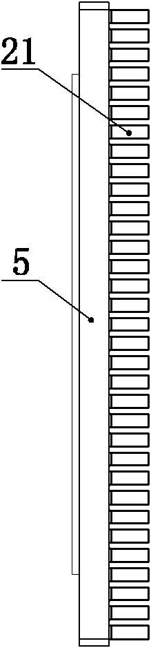
[0030] Such as figure 1 , figure 2 As shown, a CCGA560 packaged product with a pitch of 1.27 mm is assembled with a Sn10Pb90 solder column 21 with a diameter of φ0.89 mm. The post welding method of this product includes the following steps:

[0031] (1) Neatly arrange the Sn10Pb90 solder columns 21 with a diameter of φ0.89mm in the special mold 1;

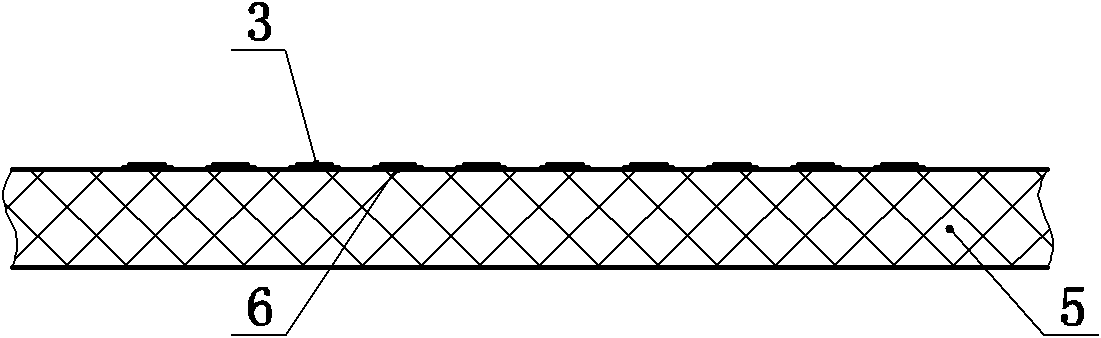
[0032] (2) Print solder paste 3 (Sn63Pb37, etc.) on the pad 6 of the substrate 5 to be planted, see image 3 ; The diameter of the solder paste 3 is: 0.89mm, and the thickness of the solder paste is: 0.20mm.

[0033] (3) Put the to-be-planted substrate 5 printed with solder paste 3 on the pad 6 into a bench-top nitrogen lead-free reflow furnace. The reflow furnace is produced by Beijing Qixing Tianyu Technology Co., Ltd., and the equipment model is TYR108N. The solder paste 3 is melted by a reflow oven, and the solder paste 3 forms a half-moon spherical crown on each pad 6, which is the convex solder 4, see Figure 4 ;The ref...

Embodiment 2

[0038] Such as Figure 7 , Figure 8 As shown, a CCGA575 packaged product with a pitch of 1.27 mm is assembled with an oxygen-free copper metal post 22 with a diameter of φ0.60 mm. The post welding method of this product includes the following steps:

[0039] (1) Neatly arrange the oxygen-free copper metal pillars 22 with a diameter of φ0.60mm in the special mold 1;

[0040] (2) Print solder paste 3 with a diameter larger than that of the metal pillar 22 on the pad 6 of the substrate 5 to be planted. The solder paste grade is such as INDIUM's IPN: 82342, the diameter of the solder paste is 0.82mm, and the thickness of the solder paste is 0.15mm. See Figure 9 ;

[0041] (3) Put the substrate 5 to be planted with the solder paste 3 printed on the pad 6 into the heating table, and melt the solder paste 3 through the heating table, and the solder paste 3 forms a half-moon spherical crown on each pad 6, That is, convex solder 4, see Figure 10 ;The melting of the heating tab...


PUM

PropertyMeasurementUnit
diameteraaaaaaaaaa
thicknessaaaaaaaaaa
diameteraaaaaaaaaa

Abstract

The invention relates to a welding method for welding columns of an encapsulated integrated circuit (IC). The welding method is characterized by comprising the following steps: tidily arranging the welding columns in a die; forming a convex welding flux on a pad of a column base plate to be embedded; placing the welding columns and the die in the pad which corresponds to a CLGA560 circuit of the column base plate to be embedded and is provided with the convex welding flux, and transferring the pad into a reflow oven so as to complete welding; and after completion of the welding operation, washing and drying. The welding method has the advantages that by virtue of factors of the convex welding flux such as point contact, solder fusing, surface tension and the like, micro-bubbles are avoided in fusion of the welding flux and an end surface so as to obtain a high-quality welding column encapsulated device without micro-bubbles on a welded surface, which solves the problem of the encapsulated micro-bubbles on the welded surface of the welding columns, saves the step of performing X-ray or ultrasonic inspection on the device so as to ensure the welding quality in the conventional welding process, and improves welding quality and welding yield.

Description

technical field [0001] The invention relates to a welding process for integrated circuit packaging pins, in particular to a welding post welding method for packaging integrated circuits, which belongs to the technical field of integrated circuit manufacturing. Background technique [0002] With the increase in the number of I / O terminals of semiconductor integrated circuit devices and the increase in packaging density, the packaging terminals are arranged in area arrays, such as ball grid arrays (BGA) and column grid arrays (CGA), and the pitch is getting more and more The smaller (2.54mm→1.27mm→1.00mm→0.80mm→...). [0003] The process method of using welding pillars to assemble and weld the required column grid array (CGA) package mainly uses printing solder paste such as silk screen or stainless steel plate or distributes solder paste with precision dispensing process, and then puts the welding pillars into the mold or puts them into the mold. After the overall welding po...

Claims


Application Information

Patent Timeline
Patent Type & Authority Applications(China)
IPC IPC(8): B23K1/00H01L21/60
Inventor 丁荣峥杨兵张顺亮
Owner WUXI ZHONGWEI GAOKE ELECTRONICS
Why Eureka
Try Eureka