Preparation method of polydimethylsiloxane micro-nanofluidic chip

A technology of polydimethylsiloxane and micro-nanofluidics, which is applied in the direction of photolithography, microstructure technology, optomechanical equipment, etc. Requirements for development, lack of simplicity of steps, repeatability and mass production of micro-nano processing alternative technologies, etc., to achieve highly repeatable results

Inactive Publication Date: 2011-08-10
NANJING UNIV
View PDF0 Cites 22 Cited by
  • Summary
  • Abstract
  • Description
  • Claims
  • Application Information

AI Technical Summary

Problems solved by technology

Some technologies based on nanowire templates or surface cracks have been developed one after another, but these technologies are basically difficult to have the flexibility in pattern design that photolithography technology has, and can only meet the preparation of relatively simple nanostructures.
And even nanolithography itself has some limitations when p

Method used


Image

  • Preparation method of polydimethylsiloxane micro-nanofluidic chip
  • Preparation method of polydimethylsiloxane micro-nanofluidic chip
  • Preparation method of polydimethylsiloxane micro-nanofluidic chip

Examples


Embodiment 1

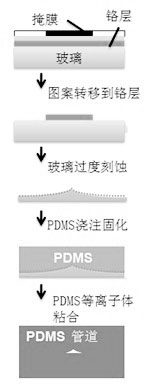
[0027] Example 1. Preparation of raised micro-nano structures on the glass surface

[0028] Step 1. In a dark room, the mask pattern is transferred to the chrome layer of the glass substrate through the UV exposure process, exposing for 0.5 minutes. Fix with a fixer (0.2% NaOH in water) for 2 minutes. Use a chrome removal solution (200g potassium dichromate and 35mL 98% acetic acid dissolved in 1L water) to remove the chrome layer outside the pattern. Remove excess photoresist with ethanol and dry.

[0029] Step 2. Put the treated glass into a constant temperature water bath (temperature 0°C), and over-etch the glass substrate with 1M etching solution for 10 hours.

[0030] Step 3. Take out the glass substrate, rinse and dry. corresponding micro-nanostructure

Embodiment 2

[0031] Example 2. Inverted mold preparation of PDMS micro-nanofluidic chip

[0032] Step 1. Mix the polydimethylsiloxane (PDMS) precursor and curing agent at a mass ratio of 3:1, pour it on the glass mold, and use a vacuum pump to remove air bubbles.

[0033] Step 2. Put the mold poured with the PDMS mixture in an oven and heat it at 40°C for 1 hour to cure the PDMS and peel it off from the glass mold.

[0034] Step 3. Treat the surface of the patterned PDMS sheet and the surface of the non-patterned PDMS substrate with oxygen plasma, and quickly attach them to obtain a polydimethylsiloxane micro-nanofluidic chip.

Embodiment 3

[0035] Example 3. Preparation of raised micro-nano structures on the glass surface

[0036] Step 1. Transfer the mask pattern to the chrome layer on the glass substrate through the UV exposure process, and expose for 5 minutes. Fix with fixer for 2 minutes. Use a chrome remover to remove the chrome layer other than the pattern. Remove excess photoresist with ethanol and dry.

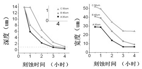
[0037] Step 2. Put the treated glass into a constant temperature water bath (temperature 40°C), and over-etch the glass substrate with 1M etching solution for 1, 2, 3 and 4 hours respectively.

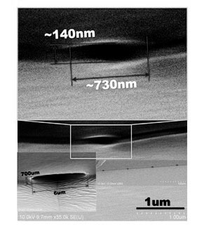
[0038]Step 3. Take out the glass substrate, rinse and dry. The corresponding micro-nano structure can be obtained, and the basic process monitoring and illustration of glass over-etching can be found in Figure 4 .


PUM


Abstract

The invention relates to a preparation method of a polydimethylsiloxane micro-nanofluidic chip. The method comprises the following steps: transferring a designed pattern of a chip structure onto a mask, closely jointing the mask with glass on which a chromium layer and a photoresist are sequentially coated, using ultraviolet light to irradiate the mask for exposure, taking out, using fixing water for fixing, using dechromisation solution to remove redundant chromium, using ethanol to remove the redundant photoresist, and completing the transfer from the designed pattern to the pattern on the chromium layer; then using etching solution to etch the glass after well processing for a certain period of time, wherein the time needs to be longer than the traditional glass etching time so as to achieve the purpose of excessive etching; taking out the well etched glass, and drying; uniformly mixing a PDMS (polydimethylsiloxane) prepolymer with a curing agent according to a certain weight ratio, uniformly distributing the mixture on a glass mold, curing for a certain period of time at the temperature of 40 DEG C-120 DEG C, and stripping off from the mold; and using oxygen and other plasmas to process a PDMS chip with the pattern and a substrate, rapidly jointing the two, forming irreversible joint, and finally getting the polydimethylsiloxane micro-nanofluidic chip.

Description

technical field [0001] The invention relates to a micro-nano fluidic chip manufacturing technology, in particular to a micro-nano fluidic chip made of a mechanically stable flexible material obtained by a micro-processing technology with a submicron-accurate structure. Background technique [0002] The research on nanofluidics emerged at the beginning of this century. Since the transport characteristics of fluids in nanotubes depend on the nanostructure and its surface properties, nanofluidics is widely used in new non-semiconductor microelectronics, biosensing, molecular manipulation, concentration and separation, fresh water There is huge potential value in processing and so on. The research on microfluidics originated in the 1990s and has developed rapidly for more than 20 years. It has attracted research forces in biology, chemistry, physics, mechanics, etc., and has developed into an integrated and efficient technical system. The functional chips that can be derived by...

Claims


Application Information

Patent Timeline
IPC IPC(8): B81C1/00G03F7/00
Inventor 徐碧漪徐静娟陈洪渊
Owner NANJING UNIV
Why Eureka
Try Eureka