Method for gettering phosphorus in N-type polysilicon slice by metallurgical method
A technology of polycrystalline silicon wafers and metallurgical methods, applied in chemical instruments and methods, silicon compounds, non-metallic elements, etc., can solve the problems of long diffusion time, high diffusion temperature, small phosphorus diffusion coefficient, etc., and achieve high surface concentration, doping High concentration and good repeatability
- Summary
- Abstract
- Description
- Claims
- Application Information
AI Technical Summary
Problems solved by technology
Method used
Image
Examples
Embodiment 1
[0031] (1) Clean metallurgical N-type polysilicon wafers with RCA liquid, and dry; RCA liquid cleaning includes: No. III liquid H 2 SO 4 :H 2 o 2 =4:1; No. I liquid NH 4 OH:H 2 o 2 :H 2 O=1:2:5; II solution HCl:H 2 o 2 :H 2 O=1:2:8. h 2 SO 4 、H 2 o 2 , NH 4 Both OH and HCl are of superior grade, and the mass fractions are 95-98%, 30%, 25-28%, and 36-38% respectively, and the three solution formulas adopt volume ratio.
[0032] (2) Pass the silicon wafer obtained in step (1) into phosphorus oxychloride POCl at a temperature of 900°C in a four-tube microcomputer diffusion furnace 3 Perform phosphorus gettering treatment for 3 hours, the gas flow rates used are: large N 2 1.5L / min; small N 2 0.05L / min; O 2 0.3L / min, the silicon wafer is naturally cooled in the air.
[0033] (3) Soak the silicon chip obtained in step (2) in dilute HF (HF: H 2 (O=1:10) solution for 10min, then HF:HNO 3(1:3) Soak in acid corrosion solution for 45s, and wash with deionized water ...
Embodiment 2
[0036] Same as embodiment 1, its difference is that phosphorus gettering heat treatment temperature and time are different, and step (2) is:
[0037] (2) Pass the silicon wafer obtained in step (1) into POCl at a temperature of 1200°C in a four-tube microcomputer diffusion furnace 3 For 2h phosphorus gettering treatment, the gas used is the flow rate: large N 2 1.5L / min; small N 2 0.05L / min; O 2 0.3L / min, the silicon wafer is naturally cooled in the air.
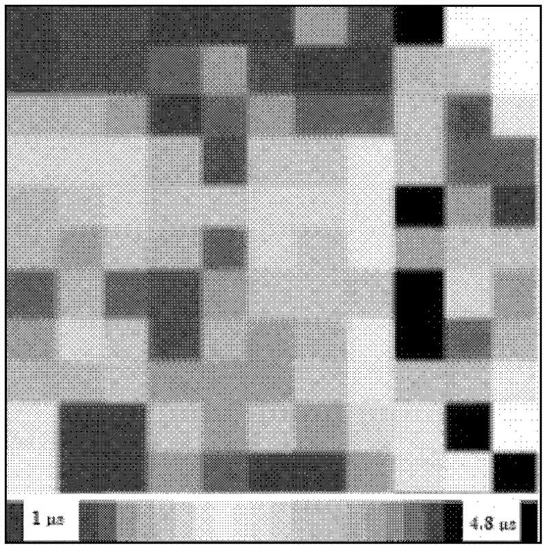
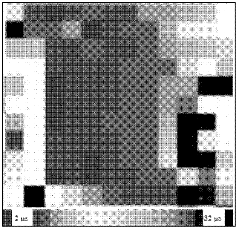
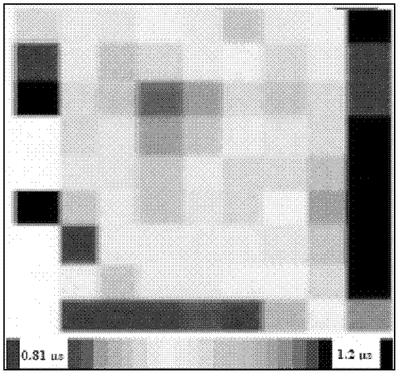
[0038] The resistivity of the silicon wafer obtained in step (3) is tested; PECVD double-sided deposition of silicon nitride 80nm measures the minority carrier lifetime of the silicon wafer. The test method is the same as in Example 1, and the results show that the average minority carrier lifetime is increased from 1.2 μs to 12.0 μs, and the minority carrier lifetime distribution diagram is as follows figure 2 As shown, the resistivity increased from 0.2Ω·cm to 1.0Ω·cm.
[0039] Minority carrier lifetime distribution ...
PUM
| Property | Measurement | Unit |
|---|---|---|
| electrical resistivity | aaaaa | aaaaa |
| thickness | aaaaa | aaaaa |
| depth | aaaaa | aaaaa |
Abstract
Description
Claims
Application Information


