Pixel array

A pixel array and pixel technology, applied in the field of pixel arrays, can solve the problems of large black matrix area and reduced aperture ratio, and achieve the effect of avoiding blocking pixel electrodes and increasing the aperture ratio

Active Publication Date: 2011-08-17
AU OPTRONICS CORP
View PDF0 Cites 7 Cited by
  • Summary
  • Abstract
  • Description
  • Claims
  • Application Information

AI Technical Summary

Problems solved by technology

[0012] However, since the known common line 160 and the capacitive lower electrode R2 of the storage capacitor 142c are all disposed below the edge of the pixel electrode 142b, the area overlapping the pixel electrode 142b is a strip with a very long edge, so black The area of ​​the matrix is ​​large, and this will cause the black matrix to cover too many pixel electrodes 142b so that the aperture ratio (aperture ratio) is reduced

Method used


Image

  • Pixel array
  • Pixel array
  • Pixel array

Examples


Embodiment Construction

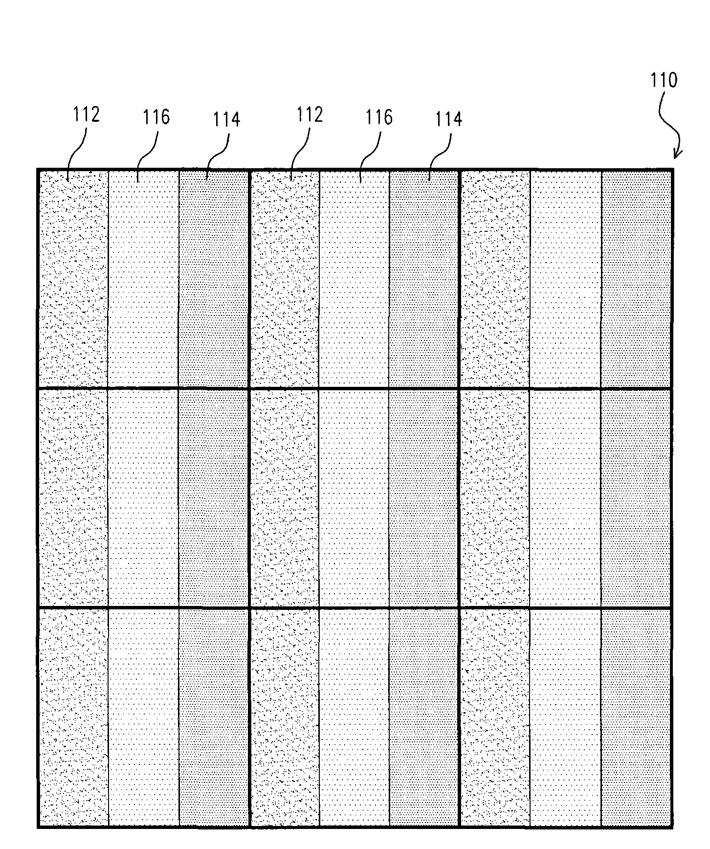
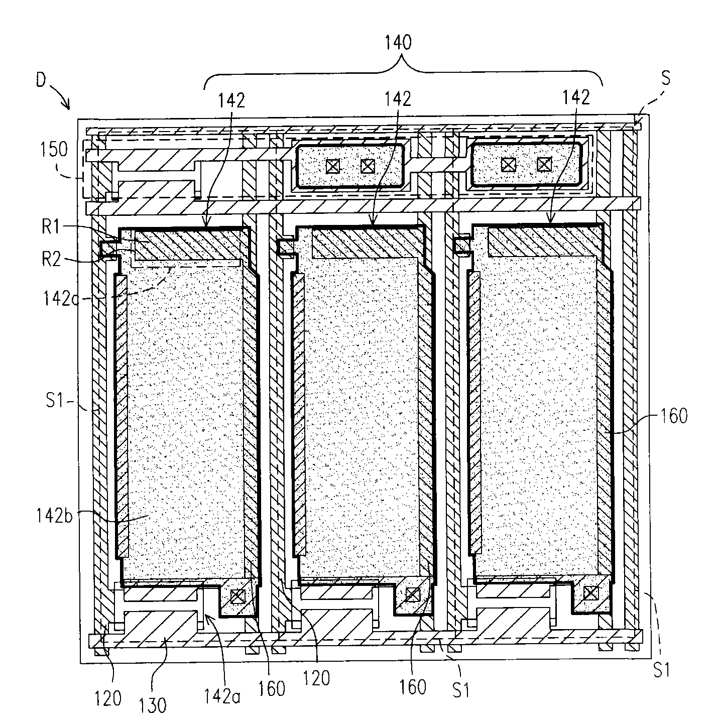
[0083] Figure 2A ~ Figure 2C A top view showing the manufacturing process of the pixel array according to an embodiment of the present invention.

[0084] It is worth noting that, for simplicity of illustration, Figure 2A ~ Figure 2C The manufacturing process of only one pixel in the pixel array is shown, and for Figure 2A ~ Figure 2C The description is only for the manufacturing process of one pixel, but it is not used to limit the number of pixels of the present invention. In other words, the pixel array of the present invention can have a plurality of pixels, and these pixels can all be Figure 2A ~ Figure 2C production method to form.

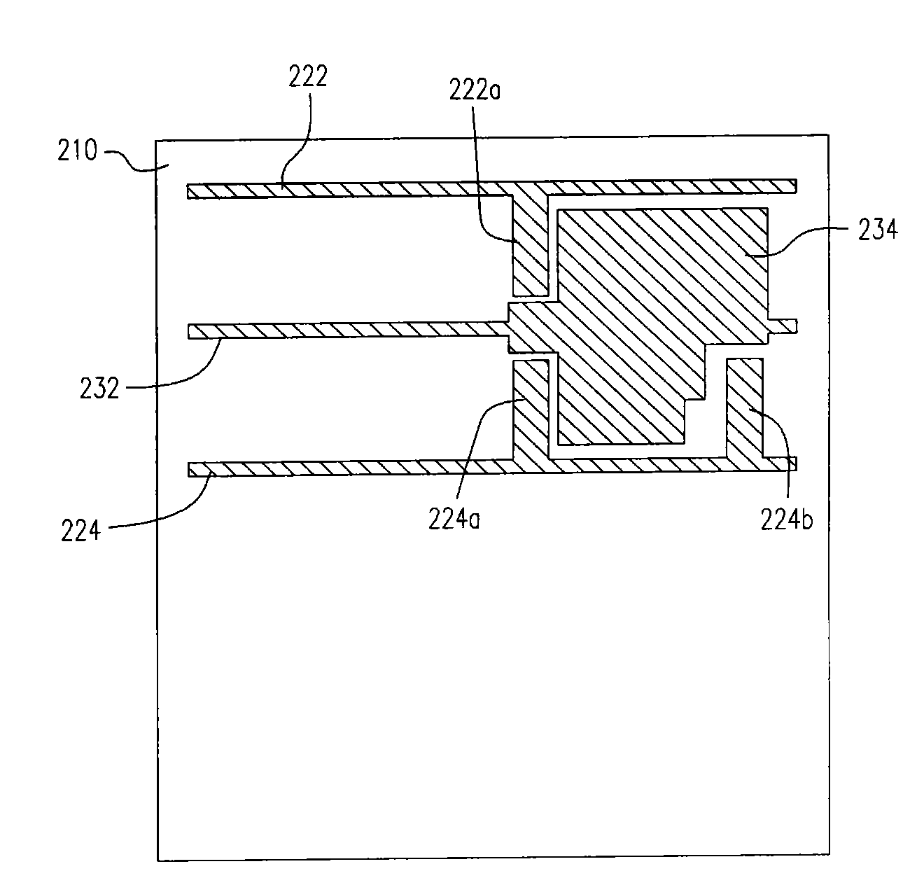
[0085] Please refer to Figure 2A A substrate 210 is provided, and a plurality of scan lines 222 , 224 parallel to each other, a common line 232 and a first capacitor electrode 234 located between the scan lines 222 , 224 are formed on the substrate 210 . The scan line 222 has a first gate terminal 222 a facing the scan line 224 , a...


PUM


Abstract

The invention provides a pixel array, which comprises multiple scanning lines, multiple data lines and multiple pixels. The data lines and the scanning lines are crossed with each other to define multiple sub pixel areas arranged in the form of an array. Each pixel is configured in a pixel area composed of m*n sub pixel areas, wherein m and n are both integers of more than 1; and each pixel comprises multiple sub pixels, wherein each sub pixel comprises an active element, a pixel electrode and a storage capacitor; and at least partial storage capacitors of each sub pixel in the same pixel areintensively configured in one of the sub pixel areas.

Description

[0001] This application is a divisional application of the patent application with application number: 201010003890.3, invention name "Pixel Array", and application date: 2010.1.15. technical field [0002] The present invention relates to a pixel array, and more particularly to a pixel array with a storage capacitor. Background technique [0003] With the rapid development and application of information technology, wireless mobile communication and information home appliances, many information products have changed from traditional input devices such as keyboards or mice in order to achieve the purpose of more convenient portability, lighter size and more humanized operation. To use the touch panel (Touch Panel) as an input device. [0004] A general touch panel is to add a film layer with touch function on the original panel. However, the manufacturing process of this type of surface-mounted touch panel requires an additional step of assembling the panel and the touch fil...

Claims


Application Information

Patent Timeline
Patent Type & Authority Applications(China)
IPC IPC(8): G02F1/1362G02F1/133G06F3/041H01L27/02
Inventor 郭威宏杨敦钧李锡烈黄伟明
Owner AU OPTRONICS CORP
Why Eureka
Try Eureka