Power factor correction circuit
A power factor correction, power stage circuit technology, applied in the power supply field, can solve the problems of miniaturization and integration of disadvantageous circuits, increase the cost of system implementation, etc., and achieve the effect of reducing anti-electromagnetic interference and realizing power factor correction.
- Summary
- Abstract
- Description
- Claims
- Application Information
AI Technical Summary
Problems solved by technology
Method used
Image
Examples
Embodiment 1
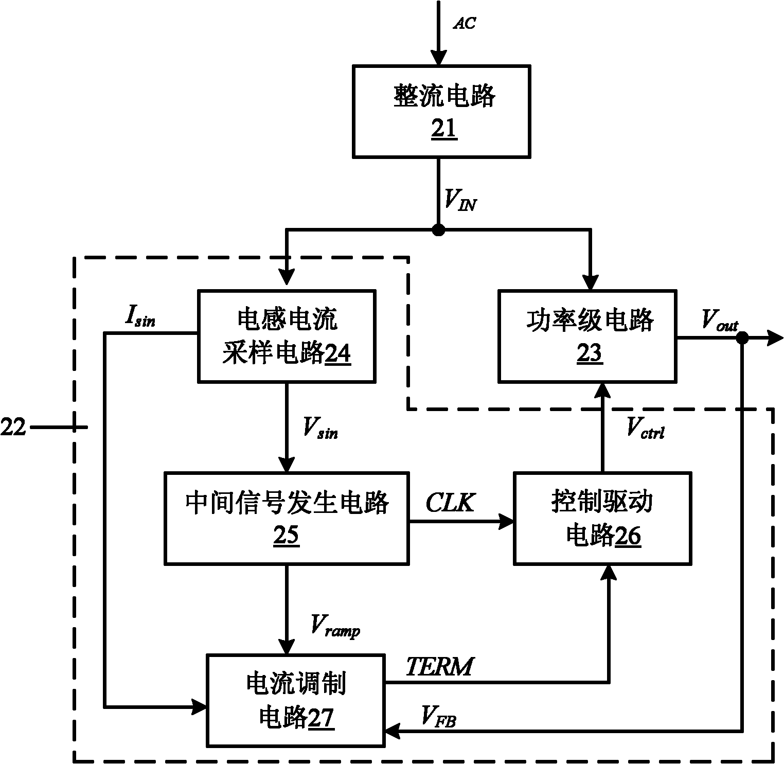
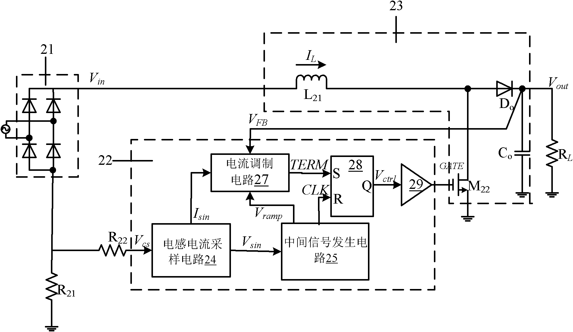
[0066] In this embodiment, the concrete idea of the present invention is described by taking the AC power supply as an example, below in conjunction with the figure image 3 , Figure 4 and Figure 5 Taking an AC / DC power supply circuit as an example of a step-up power stage circuit, the working process of the power factor correction circuit in this embodiment is described in detail, image 3 It is an AC / DC power supply circuit with a step-up power stage circuit, Figure 4 is the working waveform diagram of the power factor correction circuit in the AC / DC power supply, Figure 4 It is a schematic diagram of the circuit structure of the current modulation circuit 27.
[0067] see image 3 and Figure 4 , the working process of the whole AC / DC power supply circuit is as follows: the external sinusoidal AC input AC passes through the bridge rectifier circuit 21 to output the full upper half-cycle sinusoidal voltage V IN , flows to the inductor L 21 The inductor current I...
Embodiment 2
[0083] The power factor correction circuit and the overall circuit structure diagram of the AC / DC power supply disclosed in the embodiment of the present invention are similar to the previous embodiment, the difference is that the embodiment of the present invention discloses the structure of the inductor current sampling circuit 24 and the intermediate signal generating circuit 25 Figure, such as Image 6 and Figure 7 as shown, Image 6 It is a circuit structure diagram of the inductor current sampling circuit 24 disclosed in this embodiment, Figure 7 It is a circuit structure diagram of the intermediate signal generating circuit 25 disclosed in this embodiment, Figure 8 It is a working waveform diagram of the intermediate signal generating circuit 25.
[0084] like Image 6 As shown, the inductor current sampling circuit includes:
[0085] The first voltage-current conversion circuit 41 is used to convert the sampled voltage signal V cs Converted to a sinusoidal hal...
Embodiment 3
[0114] Different from the previous embodiment, the circuit structure diagram of the intermediate signal generating circuit in this embodiment is as follows Figure 9 As shown, the upper limit reference voltage in this embodiment is a variable upper limit voltage, therefore, the intermediate signal generating circuit 25 also includes:
[0115] A variable upper limit voltage generating circuit 56, the variable upper limit voltage generating circuit 56 includes a third reference current source I ref3 and the third resistor R 52 , the third reference current source I ref3 The first end of the access to the first reference voltage V DD , the second terminal and the third resistor R 52 connected to the first terminal, the third reference current source I ref3 with the third resistor R 52 The connection point of the access to the modulated current signal I mod , the third resistor R 52 The second end of the ground; the modulation current signal I mod with the third reference ...
PUM
 Abstract
Description
Claims
Application Information


