CMOS (Complementary Metal Oxide Semiconductor) image sensor pixel and control time sequence thereof
An image sensor and timing control technology, which is applied in image communication, radiation control devices, electric solid devices, etc., can solve the problem of low aperture ratio of metal windows, achieve the effect of improving light efficiency, aperture ratio, and image quality
- Summary
- Abstract
- Description
- Claims
- Application Information
AI Technical Summary
Problems solved by technology
Method used
Image

Examples
specific Embodiment 1
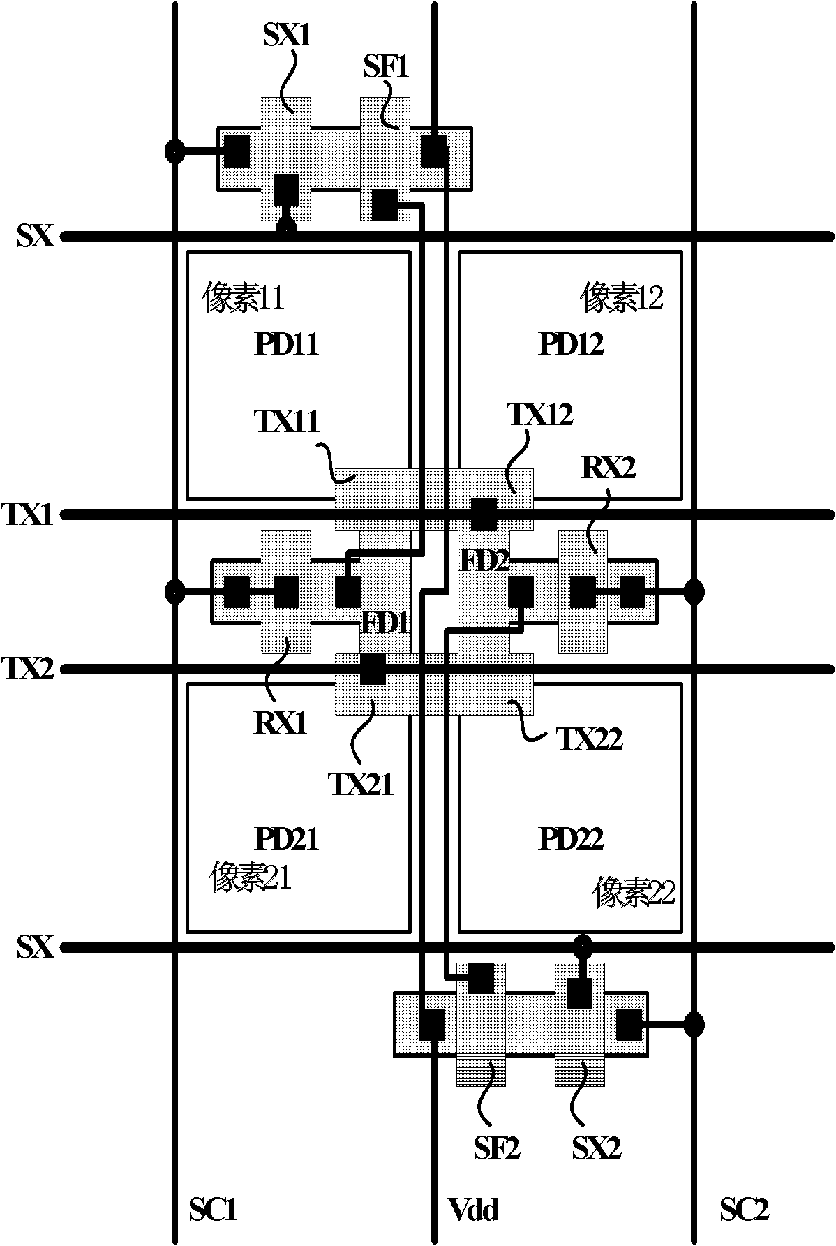
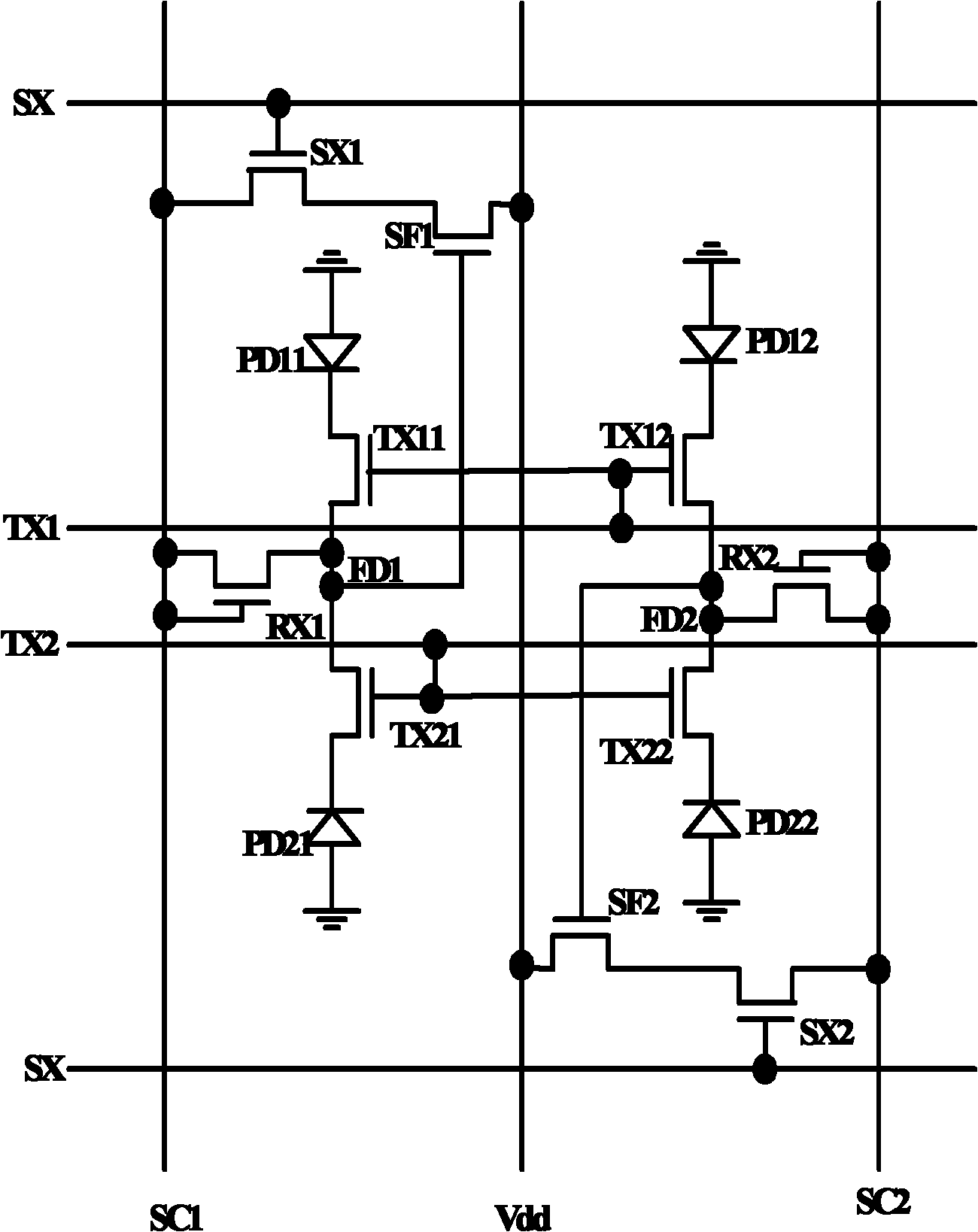
[0048] like figure 1 As shown, the CMOS image sensor pixel adopts 4T2S structure, including four pixels, and the photodiodes of pixel 11, pixel 12, pixel 21 and pixel 22 are respectively PD11, PD12, PD21 and PD22; TX11 and TX12 are respectively pixel 11 and pixel 12 TX21 and TX22 are the charge transfer transistors of pixel 21 and pixel 22 respectively; SX1, SF1 and RX1 are the select transistors, source follower transistors and reset transistors of pixel 11 and pixel 21 respectively; SX2, SF2 and RX2 are respectively Select transistors, source follower transistors and reset transistors of pixels 12 and 22 . Pixel 11 and pixel 21 share transistors SX1, SF1, RX1 and active region FD1 (Floating Diffusion), pixel 12 and pixel 22 share transistors SX2, SF2, RX2 and active region FD2; shared pixel 11 and pixel 21 share Pixel 12 and pixel 22 form a back-to-back structure in the horizontal direction.
[0049] The metal interconnection lines used by CMOS image sensor pixels are expr...
specific Embodiment 2
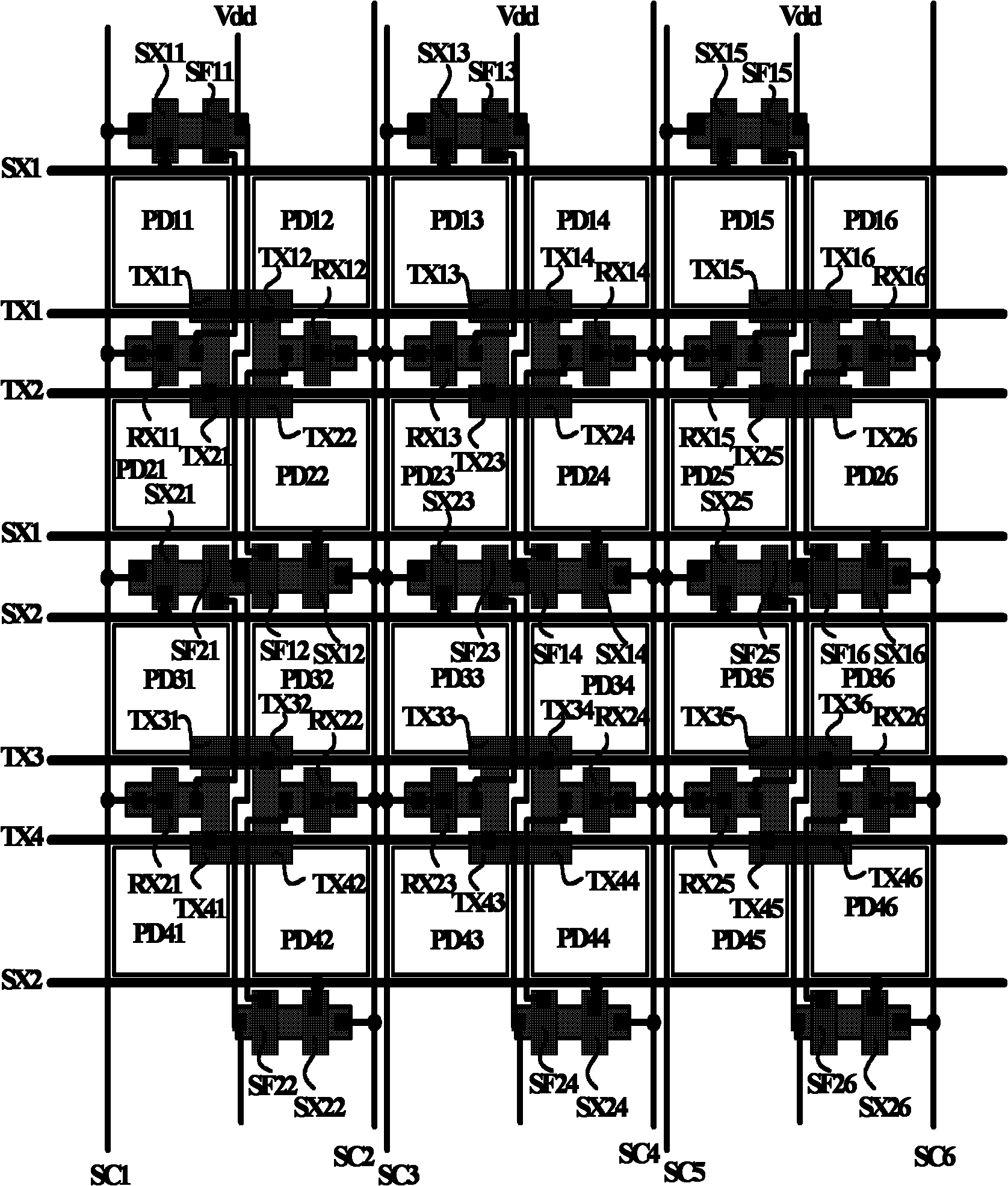
[0051] like image 3 As shown, it is a schematic diagram of a 6X4 pixel array layout; image 3 The circuit schematic diagram corresponding to the schematic diagram of the pixel array layout is as follows: Figure 4 shown.
[0052] image 3 and Figure 4 In the pixel array shown, the FD area of each pixel is connected to the gate of each corresponding source-following transistor with the first-layer metal connection, and the power supply Vdd line uses the first-layer metal connection; the SC1-SC6 lines are the first-layer metal connection, As a signal output line and a column controller timing control line. The second layer metal connection SX1 is connected to the gates of SX11~SX16, the second layer metal connection TX1 is connected to the gates of TX11~TX16, the second layer metal connection TX2 is connected to the gates of TX21~TX26; the second layer metal connection The line SX2 is connected to the gates of SX21-SX26, the second-layer metal connection TX3 is connecte...
specific Embodiment 3
[0053] The details of CMOS image sensor pixel array signal acquisition are expressed as follows:
[0054] like Figure 5 Shown is a schematic diagram of a pixel array with a row decoder and a column controller. The row decoder is placed on the left side of the pixel array (it can also be placed on the right side of the array), the column controller is placed on the top of the pixel array, and the signal readout device is placed at the bottom of the pixel array; the decoder, controller and The location of the signal readout device is not the only method of the present invention, and can also be adjusted according to the specific design and layout of the chip. Figure 5 In the schematic diagram shown, the specific positions of the array pixels are marked in detail, and the specific numbers of the timing output control lines of the decoder and the timing control lines of the column controller are also marked in detail. m and n are non-negative integers, representing the pixel r...
PUM
 Abstract
Description
Claims
Application Information
 - R&D
- Intellectual Property
- Life Sciences
- Materials
- Tech Scout
- Unparalleled Data Quality
- Higher Quality Content
- 60% Fewer Hallucinations
Browse by: Latest US Patents, China's latest patents, Technical Efficacy Thesaurus, Application Domain, Technology Topic, Popular Technical Reports.
© 2025 PatSnap. All rights reserved.Legal|Privacy policy|Modern Slavery Act Transparency Statement|Sitemap|About US| Contact US: help@patsnap.com